Check patentability & draft patents in minutes with Patsnap Eureka AI!

Silicon wafer position detection device and method

A detection device and silicon wafer technology, applied in the manufacture of electrical components, circuits, semiconductor/solid-state devices, etc., can solve the problems of complex device structure and high cost, and achieve the effects of convenient operation, low cost and simple structure

Active Publication Date: 2019-05-17
ACM RES SHANGHAI
View PDF11 Cites 0 Cited by
  • Summary
  • Abstract
  • Description
  • Claims
  • Application Information

AI Technical Summary

Problems solved by technology

[0004] Although the above-mentioned device can detect whether the position of the silicon wafer is correct, the structure of the device is too complicated and the required cost is high.

Method used


Image

  • Silicon wafer position detection device and method
  • Silicon wafer position detection device and method
  • Silicon wafer position detection device and method

Examples


Embodiment Construction

[0028] In order to describe the technical content, structural features, goals and effects of the present invention in detail, the following will be described in detail in conjunction with the embodiments and drawings.

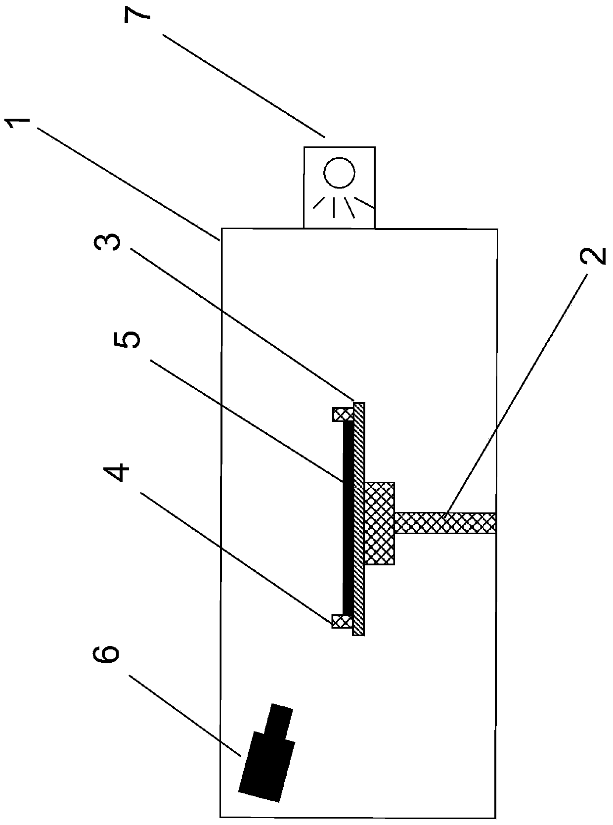
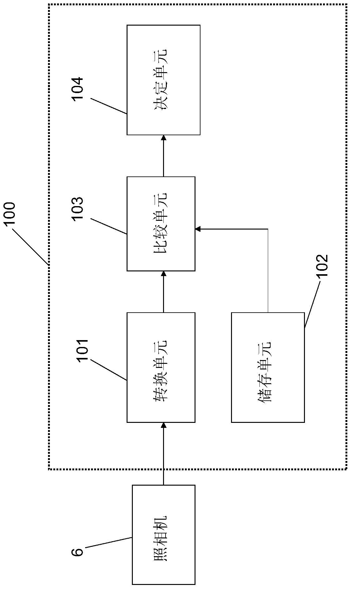
[0029] refer to figure 1 , which discloses a structural schematic diagram of an exemplary embodiment of the silicon wafer position detection device of the present invention. Such as figure 1 As shown, the device includes a process chamber 1 , a base 2 arranged in the process chamber 1 and a wafer clamp 3 arranged on the base 2 . The wafer holder 3 has several positioning pins 4 . The silicon wafer 5 is placed on the silicon wafer holder 3 . When the silicon wafer holder 3 rotates, the positioning pin 4 fixes the silicon wafer 5 on the silicon wafer holder 3 . The camera 6 is arranged at a corner of the process chamber 1 and above the silicon wafer 5. During the rotation of the silicon wafer 5 with the wafer holder 6, the camera 6 captures the edge of the ro...


PUM


Abstract

An apparatus and method for detecting position of a wafer on a chuck are disclosed. The apparatus includes a camera (6) and an image processor (100) which includes a transforming unit (101), a comparing unit (103) and a determining unit (104). The method includes the following steps: taking an image of edge of the wafer and send image data to the image processor (S23); transforming the image data into image pixels and comparing the image pixels with reference pixels (S25'), and determining whether the wafer is in position on the chuck (S26).

Description

technical field [0001] The invention relates to the field of semiconductor device manufacturing, in particular to a device and method for detecting the position of a silicon chip to detect whether the position of the silicon chip on a silicon chip holder is correct. Background technique [0002] During the manufacturing process of semiconductor devices, silicon wafers need to be transferred between various process chambers, such as film deposition chambers, etching chambers, and cleaning chambers, in order to complete the corresponding process processing. In order to improve the processing efficiency and meet the requirements of a higher process environment, a manipulator is used to transfer silicon wafers. Usually, the silicon wafer is placed on the silicon wafer holder in the process chamber by the manipulator for process processing, and whether the silicon wafer can be accurately placed on the preset position of the silicon wafer holder will have a greater impact on the p...

Claims


Application Information

Patent Timeline
Patent Type & Authority Patents(China)
IPC IPC(8): H01L21/68
CPCH01L21/67259H01L21/681
Inventor 王坚赵宇黄玉峰陈福发王晖
Owner ACM RES SHANGHAI
Features
  • R&D
  • Intellectual Property
  • Life Sciences
  • Materials
  • Tech Scout
  • Unparalleled Data Quality
  • Higher Quality Content
  • 60% Fewer Hallucinations
Learn More