A touch panel and manufacturing method thereof and a display device

A technology for a touch panel and a manufacturing method, which are applied in the fields of semiconductor/solid-state device manufacturing, instruments, and electric solid-state devices, etc., can solve the problems of high production cost, many process processes, electromagnetic interference of touch-control structures and display structures, etc. The effect of production cost, reduction of process and improvement of touch effect and display effect

Active Publication Date: 2015-03-11
WUHAN TIANMA MICRO ELECTRONICS CO LTD +1
View PDF5 Cites 36 Cited by
  • Summary
  • Abstract
  • Description
  • Claims
  • Application Information

AI Technical Summary

Problems solved by technology

[0004] In view of this, an embodiment of the present invention provides a touch panel, a manufacturing method thereof, and a display device to solve the problem of using On-Cell to manufacture an AMOLED display panel with a touch function in the prior art, and the difference between the touch structure and the display structure. Electromagnetic interference will be generated during the production process, as well as technical problems such as many processes and high production costs in the production process

Method used


Image

  • A touch panel and manufacturing method thereof and a display device
  • A touch panel and manufacturing method thereof and a display device
  • A touch panel and manufacturing method thereof and a display device

Examples


Embodiment Construction

[0042] The present invention will be further described in detail below in conjunction with the accompanying drawings and embodiments. It should be understood that the specific embodiments described here are only used to explain the present invention, but not to limit the present invention. In addition, it should be noted that, for the convenience of description, only parts related to the present invention are shown in the drawings but not all content.

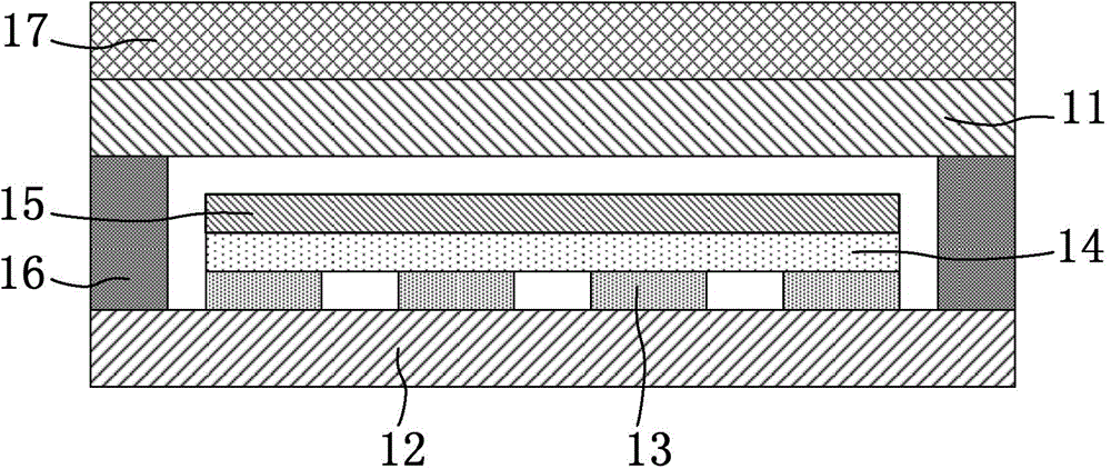
[0043] With the development of display technology, a touch structure will be integrated in the AMOLED display panel to realize the touch function. In the prior art, in order to realize the touch function of the AMOLED display panel, the touch control structure is integrated with the AMOLED display structure in the form of On-Cell.

[0044] Figure 1a It is a structural schematic diagram of an AMOLED display panel in the prior art. Such as Figure 1a As shown, the AMOLED display panel includes: a first substrate 11 and a secon...


PUM


Abstract

The invention discloses a touch panel and manufacturing method thereof and a display device, wherein the touch panel comprises: a first substrate and a second substrate oppositely disposed; an organic light emitting layer located between the first substrate and the second substrate, wherein the organic light emitting layer includes at least a cathode layer formed by a plurality of strip-like cathode electrodes; and a first touch layer located between the first substrate and the second substrate, wherein the first touch layer comprises a plurality of first touch electrodes, the first touch electrode comprises at least one first touch sub electrode the projection on the organic light emitting layer of which is located between two adjacent cathode electrodes. The technical solution of the invention can reduce at least electromagnetic interference between the first touch layer and the cathode electrode, and thus can improve the touch effect and the display effect. In addition, the invention can further reduce manufacture procedure of the process and reduce product costs.

Description

technical field [0001] The invention relates to the field of display technology, in particular to a touch panel, a manufacturing method thereof, and a display device. Background technique [0002] AMOLED (Active Matrix Organic Light Emitting Diode, active matrix organic light-emitting diode) has the characteristics of self-illumination, low power consumption, fast response speed, high contrast and wide viewing angle. Therefore, AMOLED has a wide range of applications in the field of display technology. Application prospects. [0003] With the development of display technology, a touch structure will be integrated in the AMOLED display panel to realize the touch function. In the prior art, in order to realize the touch function of the AMOLED display panel, the touch control structure is integrated with the AMOLED display structure in the form of On-Cell. However, for the AMOLED display panel produced in this integrated form, when the display panel is working, electromagneti...

Claims


Application Information

Patent Timeline
Patent Type & Authority Applications(China)
IPC IPC(8): H01L27/32H01L51/52H01L51/56G06F3/041
CPCG06F3/0412G06F2203/04103G06F3/0445G06F3/0446G06F3/0443H10K59/40
Inventor 熊志勇姚绮君钱栋
Owner WUHAN TIANMA MICRO ELECTRONICS CO LTD
Why Eureka
Try Eureka