Light-emitting diode unit and light-emitting device

A technology for light-emitting diodes and light-emitting devices, which is applied to electrical components, electrical solid-state devices, circuits, etc., can solve the problems of increasing the electrode area, reducing the light-emitting area of ​​the light-emitting diode die, and complicated circuit configuration steps of the light-emitting diode die array. The effect of reducing the electrode area and increasing the effective light-emitting area

Inactive Publication Date: 2015-03-18
ASDA TECH
View PDF5 Cites 0 Cited by
  • Summary
  • Abstract
  • Description
  • Claims
  • Application Information

AI Technical Summary

Problems solved by technology

Since in the flip-chip process, the electrodes connected to the circuit board need a certain area to set a sufficient size of solder, the design of the application to connect the electrodes of each die to the circuit board will lead to an increase in the electrode area and a reduction in the area of ​​the electrode. The light-emitting area of ​​the light-emitting diode die, and the circuit configuration steps of the light-emitting diode die array are too complicated

Method used


Image

  • Light-emitting diode unit and light-emitting device
  • Light-emitting diode unit and light-emitting device
  • Light-emitting diode unit and light-emitting device

Examples


no. 1 example

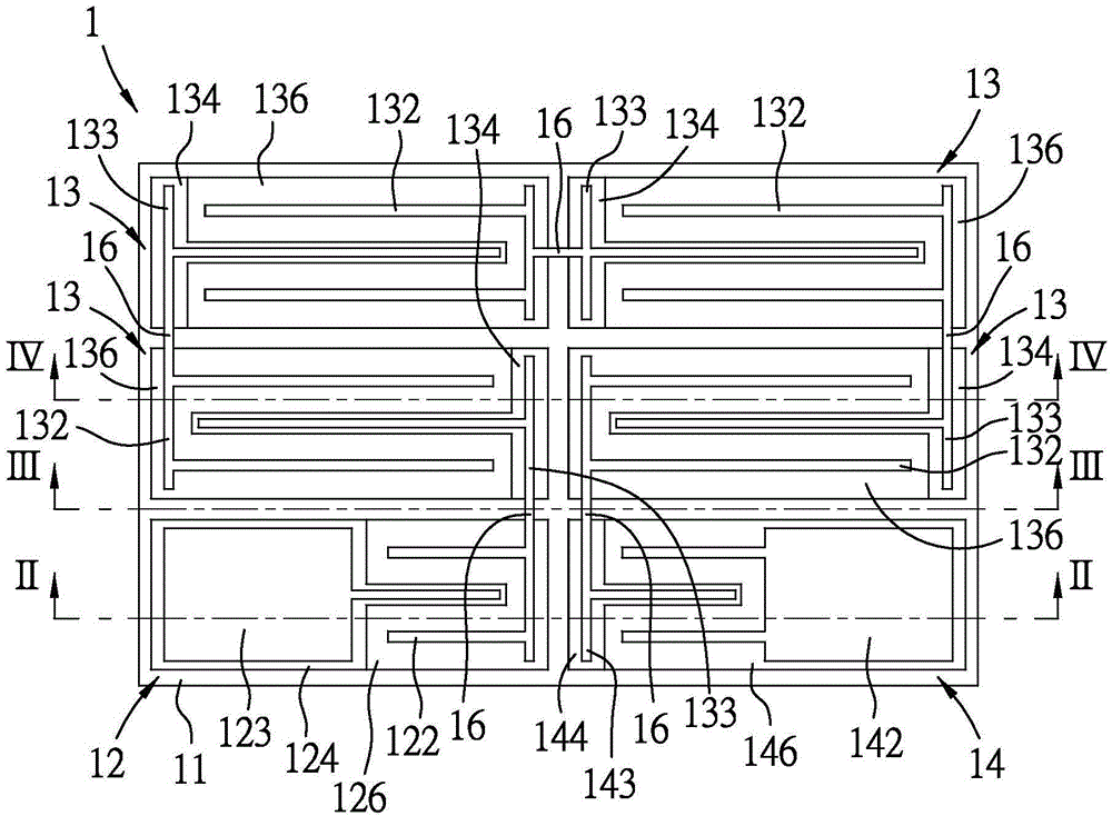
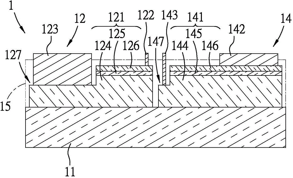
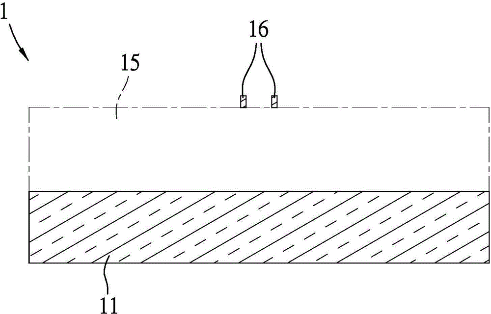
[0047] refer to Figure 1 to Figure 4 , is the first preferred embodiment of the LED unit 1 of the present invention. In this embodiment, the LED unit 1 adopts LED chip array technology, contains multiple LED chips, and can be integrated and used as a single light source.

[0048] Specifically, in the first embodiment, the LED unit 1 can radiate light in all directions, and includes a light-transmissible substrate 11, a first grain structure 12, at least one second grain structure 13, a first Three grain structures 14 , a first insulating structure 15 and a plurality of connecting portions 16 . Hereinafter, it is assumed that the light-emitting diode unit 1 can emit blue light, so its material is described with a blue light-emitting diode as an example, but the structure, material and emission color of the light-emitting diode unit 1 can be adjusted as required, for example, gallium arsenide (GaAs ), gallium arsenide phosphide (GaAsP), gallium arsenide arsenide (GaAlAs), gal...

no. 2 example

[0073] refer to figure 2 , Figure 10 , Figure 11 and Figure 12 , is the second preferred embodiment of the LED unit 1 of the present invention. in, figure 2 , Figure 11 and Figure 12 respectively Figure 10 Schematic cross-sectional view of the II-II line, the XI-XI line and the XII-XII line. Here, the light emitting diode unit 1 is different from the first embodiment in that it is a single-side light-emitting light source, and its light irradiation is generally caused by the light generated by the light-emitting diode crystal grains passing through the substrate 11, which is visually similar to that from the bottom surface of the substrate 11. To emit light, and compared with the first preferred embodiment, the light emitting diode unit 1 further includes a second insulating structure 17 and a light reflecting structure 18 .

[0074] Specifically, in this embodiment, the second insulating structure 17 is light-transmitting and covers at least the surface of the...

no. 3 example

[0077] refer to Figure 13 to Figure 16 , is the third preferred embodiment of the LED unit 1 of the present invention. Here, the light-emitting diode unit 1 is also used as a single-sided light-emitting light source, but the direction of light irradiation is opposite to that of the second embodiment, mainly emitting light from the die side. In terms of structure, compared with the first embodiment, the light emitting diode unit 1 of the third embodiment further includes a structure disposed on the substrate 11 opposite to the first grain structure 12, the second grain structure 13 and the third grain structure 14 The light reflective structure 18 on the other side, the light reflective structure 18 may be the aforementioned metal reflective structure or Bragg reflective structure. Accordingly, after the light emitted by the first grain structure 12, the second grain structure 13 and the third grain structure 14 is reflected by the reflective structure 18, it will be irradiat...


PUM

PropertyMeasurementUnit
areaaaaaaaaaaa

Abstract

The invention relates to a light-emitting diode unit, which comprises a substrate, a first crystalline grain structure, at least one second crystalline grain structure and a third crystalline grain structure. The first crystalline grain structure, the second crystalline grain structure and the third crystalline grain structure are separately arranged on the substrate, the first crystalline grain structure comprises a first positive electrode and a first negative electrode, the second crystalline grain structure comprises a second positive electrode and a second negative electrode, and the third crystalline grain structure comprises a third positive electrode and a third negative electrode. The first crystalline grain structure, the second crystalline grain structure and the third crystalline grain structure are sequentially connected in series, moreover, the area of the third positive electrode is far larger than the areas of the second positive electrode and the first positive electrode, the area of the first negative electrode is far larger than the areas of the third negative electrode and the second negative electrode, consequently, a user can conveniently carry out line configuration for the light-emitting diode unit by means of the first negative electrode and the third positive electrode, and the effective light-emitting area of the light-emitting diode unit also can be enlarged.

Description

technical field [0001] The invention relates to a light emitting diode unit and a light emitting device, in particular to a light emitting diode unit and a light emitting device with a special electrode design. Background technique [0002] A light emitting diode (LED for short) is a common semiconductor lighting component at present, and has been widely used in various application fields. As different degrees of point light, the dies of light-emitting diodes can be divided into small-sized dies (such as those with a side length of hundreds of microns) and large-sized dies (such as those with a side length of more than one millimeter). Crystal grains), although the increase in grain size can provide a larger light-emitting area, but it is accompanied by the problems of pass rate, heat dissipation and light efficiency of large-sized grains. Therefore, although there are crystal grains with a side length of about 1.5 mm (ie, 60 mil, 1 mil is about 25 microns), LED grains with...

Claims


Application Information

Patent Timeline
Patent Type & Authority Applications(China)
IPC IPC(8): H01L27/15H01L33/38
Inventor 林柏廷
Owner ASDA TECH
Why Eureka
Try Eureka