Novel wafer-level mems chip packaging structure and packaging method

A chip packaging structure and wafer-level technology, applied in the direction of microstructure devices, manufacturing microstructure devices, microstructure technology, etc., can solve the problem of limited operable space of MEMS chips and achieve the effect of large operable space

Active Publication Date: 2016-05-18
HUATIAN TECH KUNSHAN ELECTRONICS
View PDF7 Cites 0 Cited by
  • Summary
  • Abstract
  • Description
  • Claims
  • Application Information

AI Technical Summary

Problems solved by technology

At present, in the packaging process of MEMS chips, the common structure is to use glass or silicon as the cover plate, and perform packaging processes such as grinding, drilling, circuit making, and ball planting on the back of the MEMS chip. However, because the MEMS chip contains a cavity inside, for The height of the MEMS chip after grinding has a certain limit, so that in the subsequent packaging process, the operable space on the back of the MEMS chip is limited, so that such a packaging structure is limited to chips with fewer lines and simple functions.

Method used


Image

  • Novel wafer-level mems chip packaging structure and packaging method
  • Novel wafer-level mems chip packaging structure and packaging method
  • Novel wafer-level mems chip packaging structure and packaging method

Examples


Embodiment Construction

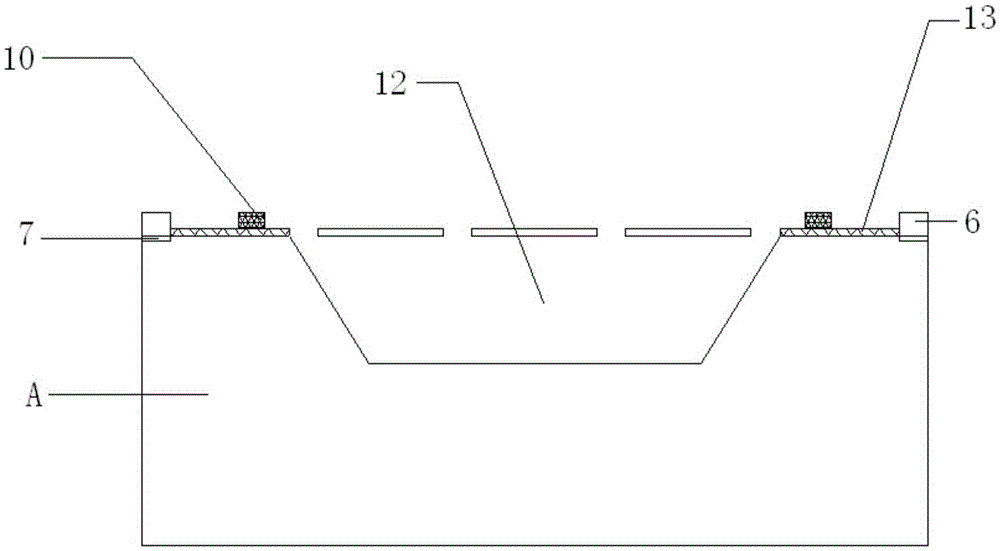
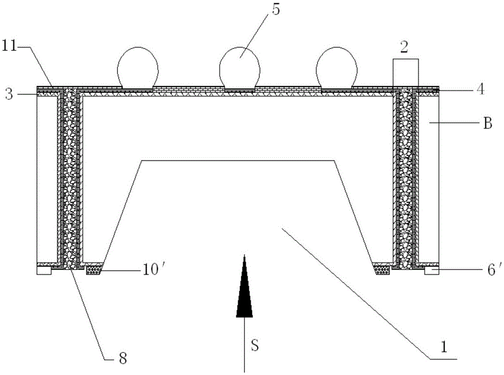
[0041] like Figure 4 As shown, a new type of wafer-level MEMS chip packaging structure, including MEMS chip A and covering silicon plate B.

[0042] see figure 1, the front middle part of the MEMS chip has a cavity 12, and several PIN pins 7 are arranged on the front periphery of the MEMS chip, and a layer of first layer is covered on the front of the MEMS chip except the cavity and the PIN pins. Insulating layer 13, the first insulating layer is used to isolate the silicon on the MEMS chip to prevent short circuit. The material of the first insulating layer can be inorganic non-metallic material, such as silicon dioxide, or a polymer insulating material, such as photolithography Glue etc. The first insulating layer is provided with a first sealing ring 10 with a set width and a set height located on the periphery of the cavity, and a first metal bump 6 is made on each of the PIN pins; usually the first The width of a sealing ring is more than 10 μm, and the first sealing ...


PUM


Abstract

The invention discloses a novel wafer-level MEMS chip packaging structure and a packaging method thereof. The packaging structure includes a MEMS chip and a covering silicon plate. The front of the MEMS chip and the front of the covering silicon plate use a sealing ring and several A metal bump bonding connection for electrically connecting the PIN pin of the MEMS chip; a wiring circuit is arranged on the back side of the covering silicon board, and a conductive through hole corresponding to the metal bump is arranged on the periphery of the covering silicon board, and the conductive through hole is located at Between the sealing ring and the metal bump, the conductive via hole electrically connects the metal bump and the wiring circuit. The packaging structure of the present invention cleverly transplants the packaging process to the covering silicon board, avoiding the processing on the back of the MEMS chip, so that the operable space is larger, and the more complex MEMS chip can be stably electrically conducted and conveniently Quick and easy packaging.

Description

technical field [0001] The invention relates to the field of wafer-level packaging of semiconductor MEMS chips, in particular to a novel wafer-level MEMS chip packaging structure and a packaging method thereof with a silicon cover plate having conductive through holes, indentations and rewiring circuits. Background technique [0002] MEMS (Micro-Electro-Mechanical Systems) chip packaging is a new packaging field, and its chips are mainly used in sensors. At present, in the packaging process of MEMS chips, the common structure is to use glass or silicon as the cover plate, and carry out the packaging process on the back of the MEMS chip, such as grinding, drilling, making circuits, and planting balls. However, because the MEMS chip contains a cavity inside, for The height of the MEMS chip after grinding has a certain limit, so in the subsequent packaging process, the operable space on the back of the MEMS chip is limited, so that such a packaging structure is limited to chips...

Claims


Application Information

Patent Timeline
Patent Type & Authority Patents(China)
IPC IPC(8): B81B7/02B81C1/00
Inventor 万里兮韩磊王晔晔范俊沈建树张春艳黄小花戴青廖建亚钱静娴王刚卢梦泽夏文斌
Owner HUATIAN TECH KUNSHAN ELECTRONICS
Why Eureka
Try Eureka