

Silicon-based microring polarization demultiplexer
A demultiplexer and micro-ring technology, applied in the field of integrated optics, to achieve the effects of reliability assurance, high reliability, and increased capacity
- Summary
- Abstract
- Description
- Claims
- Application Information
AI Technical Summary
Problems solved by technology
Method used
Image

Examples
Embodiment Construction
[0030] The present invention will be further explained below in conjunction with the accompanying drawings.
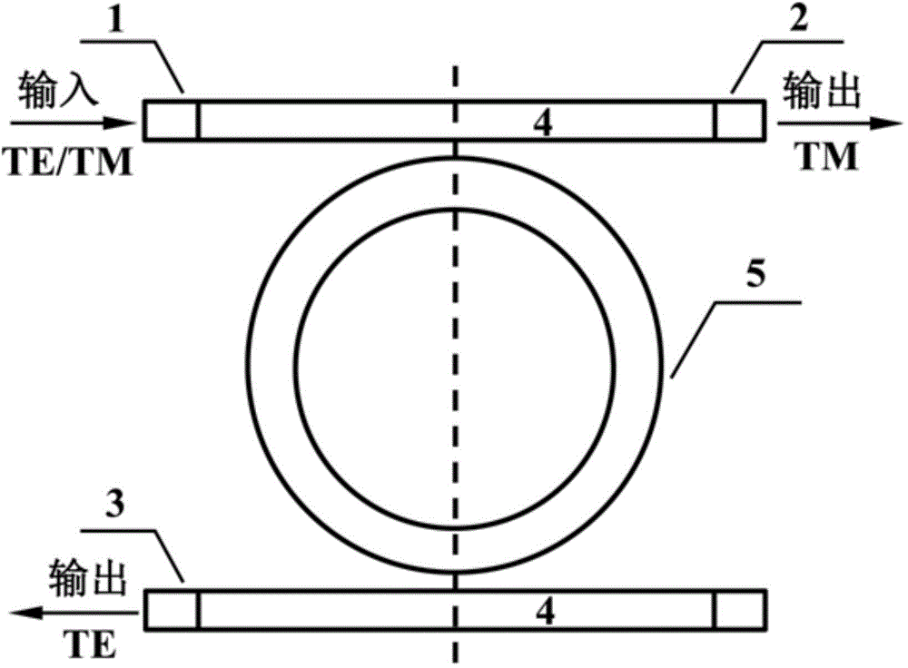
[0031] like figure 1 figure 2 As shown, a silicon-based microring polarization demultiplexer includes a silicon substrate 6 and a cladding 7, and is characterized in that it includes an input waveguide 1, a transverse magnetic mode output waveguide 2, a transverse electric mode output waveguide 3, and a mixed plasma Bulk waveguide 4 and microring 5;
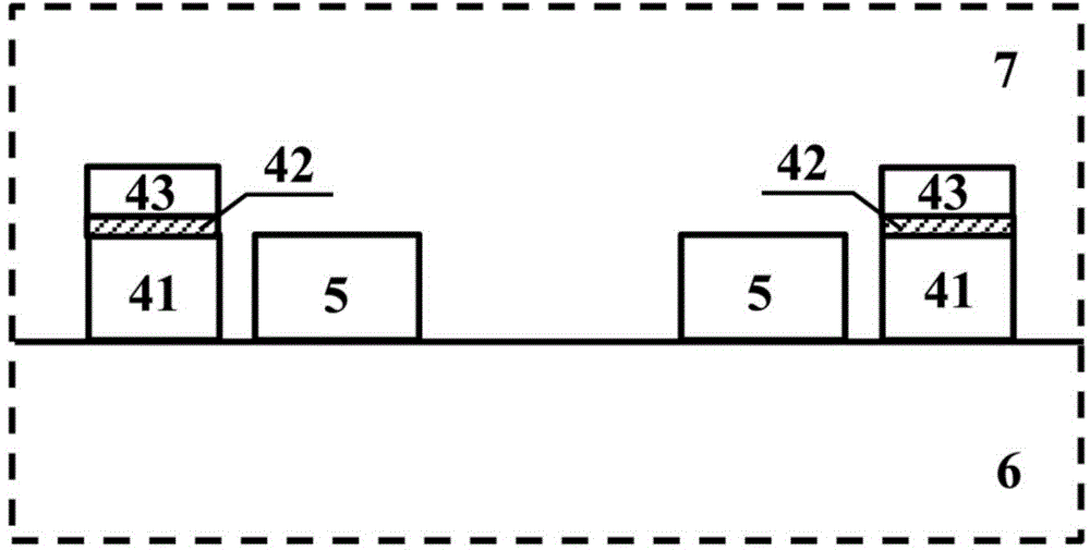
[0032] The substrate 6 is located at the inner bottom of the cladding 7, and the hybrid plasmonic waveguide 4 and the microring 5 are located on the surface of the substrate 6;
[0033] The hybrid plasmonic waveguide 4 sequentially includes a dielectric waveguide 41, a filling layer 42 and a metal covering layer 43 from bottom to top; the dielectric waveguide 41 is closely attached to the substrate 6;
[0034] The input waveguide 1 is connected to the transverse magnetic mode output waveguide 2 through the hybrid plas...
PUM
 Abstract
Description
Claims
Application Information