

Pixel array, manufacturing method thereof and display device
A technology of a pixel array and a manufacturing method, which is applied in the field of display, can solve problems affecting the display stability of an electrowetting display device, reduce the size of a storage capacitor in a pixel area, and break an ITO transparent electrode, and achieve pixel aperture ratio and enhanced storage. Capacitance, the effect of achieving stability
- Summary
- Abstract
- Description
- Claims
- Application Information
AI Technical Summary
Problems solved by technology
Method used
Image

Examples
Embodiment 1
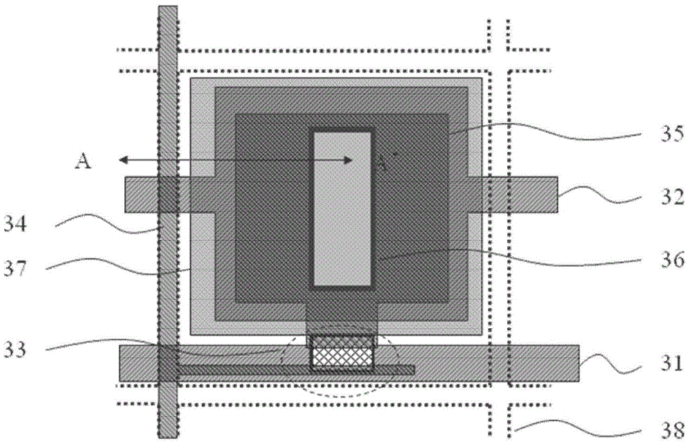
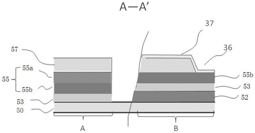
[0036] Figure 3A It is a schematic diagram showing a photolithography process in a method for fabricating a pixel array according to an embodiment of the present invention; Figure 3B It is a schematic diagram showing the secondary photolithography process in the method for manufacturing the pixel array in the above-mentioned embodiment of the present invention. Such as Figure 3A , 3B As shown, Embodiment 1 of the present invention proposes a method for manufacturing a pixel array, which specifically includes the following steps: providing a substrate 50, on which are sequentially formed: a first metal layer, a gate insulating layer and a semiconductor layer 53, a second The metal layer 55, wherein the second metal layer 55 is exposed twice and etched twice to form a first area A of the data line and a second area B of the first pixel electrode. Specifically, the manufacturing method uses physical vapor deposition PVD technology to continuously form Ti metal and Al metal ...
Embodiment 2
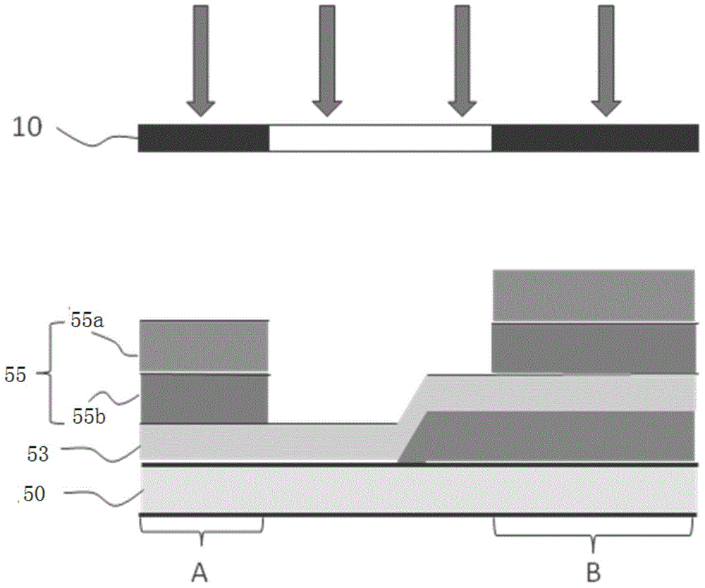
[0040] Figure 4 It is a schematic diagram of a photolithography process in a method for manufacturing a pixel array according to another embodiment of the present invention. Such as Figure 4 As shown, Embodiment 2 of the present invention proposes a method for manufacturing a pixel array, which specifically includes the following steps: providing a substrate 50, on which are sequentially formed: a first metal layer, a gate insulating layer and a semiconductor layer 53, a second The metal layer 55, wherein, the second metal layer 55 is etched twice through one exposure to form the first area A of the data line and the second area B of the first pixel electrode.
[0041] Specifically, the manufacturing method uses physical vapor deposition PVD technology to continuously form Ti metal and Al metal films to form the second metal layer. Then, the second metal layer on the data line in the first region A forms a Ti / Al structure by using the grayscale third mask 20 once for expos...
PUM
 Abstract
Description
Claims
Application Information