Manufacturing method of semiconductor device

A manufacturing method and semiconductor technology, applied in semiconductor devices, semiconductor/solid-state device manufacturing, electric solid-state devices, etc., to achieve the effects of improving electrical properties, increasing driving current, and increasing carrier mobility

Active Publication Date: 2018-06-01
SEMICON MFG INT (SHANGHAI) CORP
View PDF3 Cites 0 Cited by
  • Summary
  • Abstract
  • Description
  • Claims
  • Application Information

AI Technical Summary

Problems solved by technology

[0005] The application of embedded germanium silicon and embedded silicon carbon technology can improve the carrier mobility of semiconductor devices to a certain extent, but in practical applications, it is found that there are still problems to be solved in the manufacturing process of semiconductor devices

Method used


Image

  • Manufacturing method of semiconductor device
  • Manufacturing method of semiconductor device
  • Manufacturing method of semiconductor device

Examples


Embodiment Construction

[0030] It can be seen from the background art that there are still problems to be solved in the formation process of semiconductor devices in the prior art.

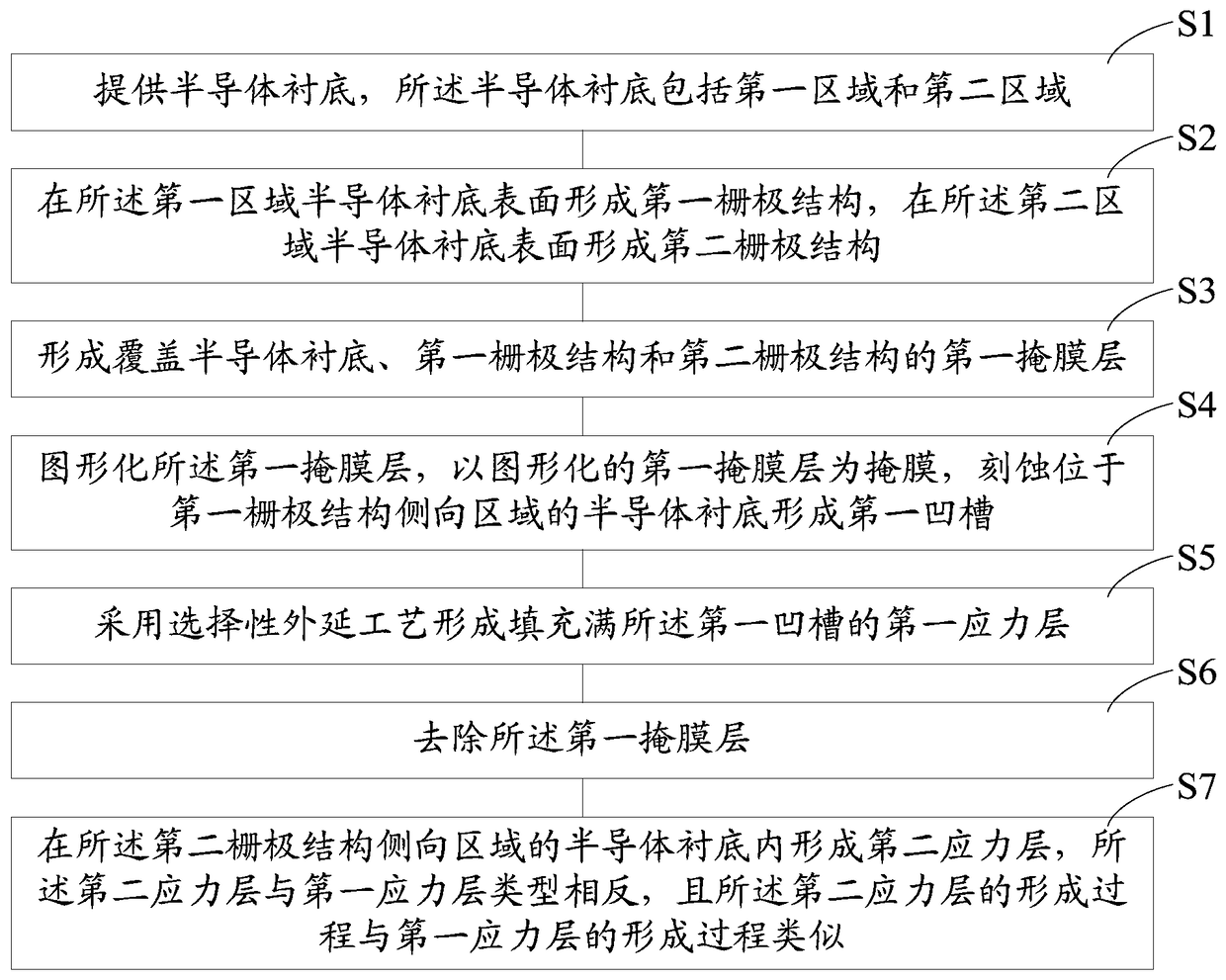
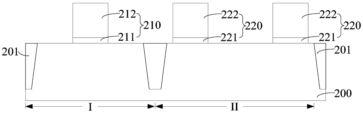
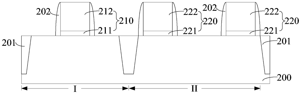
[0031] According to the research on the formation process of semiconductor devices, it is found that the formation process of semiconductor devices includes the following steps, please refer to figure 1 : Step S1, providing a semiconductor substrate, the semiconductor substrate includes a first region and a second region; Step S2, forming a first gate structure on the surface of the semiconductor substrate in the first region, and forming a semiconductor substrate in the second region A second gate structure is formed on the surface of the substrate, and there are offset spacers on both sides of the first gate structure and the second gate structure; step S3, forming a covering semiconductor substrate, the first gate structure and the second gate structure The first mask layer of the pole structure; step S4, patterning t...


PUM


Abstract

A method for making a semiconductor device comprises the following steps: providing a semiconductor substrate of which the surface is provided with gate structures; forming a mask layer covering the semiconductor substrate and the gate structures; oxidizing the mask layer to convert part of the mask layer in the thickness direction into an oxidation layer; patterning the mask layer and the oxidation layer, and etching the semiconductor substrate in the lateral regions of the gate structures with the patterned mask layer and the patterned oxidation layer as a mask to form grooves; and forming a stress layer filling the grooves. According to the method for making a semiconductor device provided by the invention, after oxidation of the mask layer, the selectivity of the process for forming the stress layer is improved, the material of the stress layer is prevented from being formed on the surface of the mask layer when the stress layer is formed, and the electrical performance of the semiconductor device is optimized.

Description

technical field [0001] The invention relates to the field of semiconductor manufacturing, in particular to a manufacturing method of a semiconductor device. Background technique [0002] With the continuous development of semiconductor technology, carrier mobility enhancement technology has been widely studied and applied. Improving the carrier mobility in the channel region can increase the driving current of MOS devices and improve the performance of the devices. [0003] In the existing manufacturing process of semiconductor devices, since stress can change the energy gap and carrier mobility of silicon materials, it has become more and more common means to improve the performance of semiconductor devices through stress. Specifically, by properly controlling the stress, the mobility of carriers (electrons in NMOS devices, holes in PMOS devices) can be increased, thereby increasing the driving current, thereby greatly improving the performance of semiconductor devices. ...

Claims


Application Information

Patent Timeline
Patent Type & Authority Patents(China)
IPC IPC(8): H01L21/336
CPCH01L27/0928H01L29/66477H01L29/7848
Inventor 何有丰何永根
Owner SEMICON MFG INT (SHANGHAI) CORP
Why Eureka
Try Eureka