Method for removing welding spots

A technology of solder joints and solder pads, applied in the field of semiconductor manufacturing, can solve the problems of low operating cost, low operating technical requirements, and small design application field limitations, so as to avoid damage and achieve the effect of secondary utilization.

Inactive Publication Date: 2015-03-25
SHANGHAI HUALI MICROELECTRONICS CORP
View PDF6 Cites 1 Cited by
  • Summary
  • Abstract
  • Description
  • Claims
  • Application Information

AI Technical Summary

Problems solved by technology

[0008] This patent is applied to the removal of solder joints when re-soldering is necessary due to inaccurate welding positions. This solution has high removal efficiency, low operating technical requirements, and low overall operating costs, but it has been accepted in the field of small design applications. limitations, so the above devices are not suitable for widespread use in small design applications

Method used


Image

  • Method for removing welding spots
  • Method for removing welding spots
  • Method for removing welding spots

Examples


Embodiment Construction

[0032] The invention provides a method for removing solder joints, which can be applied to processes with technology nodes of 90nm, 65 / 55nm, 45 / 40nm, 32 / 28nm, greater than or equal to 130nm and less than or equal to 22nm; it can be applied to the following technical platforms: Logic, Memory, RF, HV, Analog / Power, MEMS, CIS, Flash, eFlash, and Package.

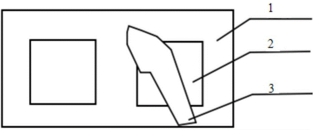
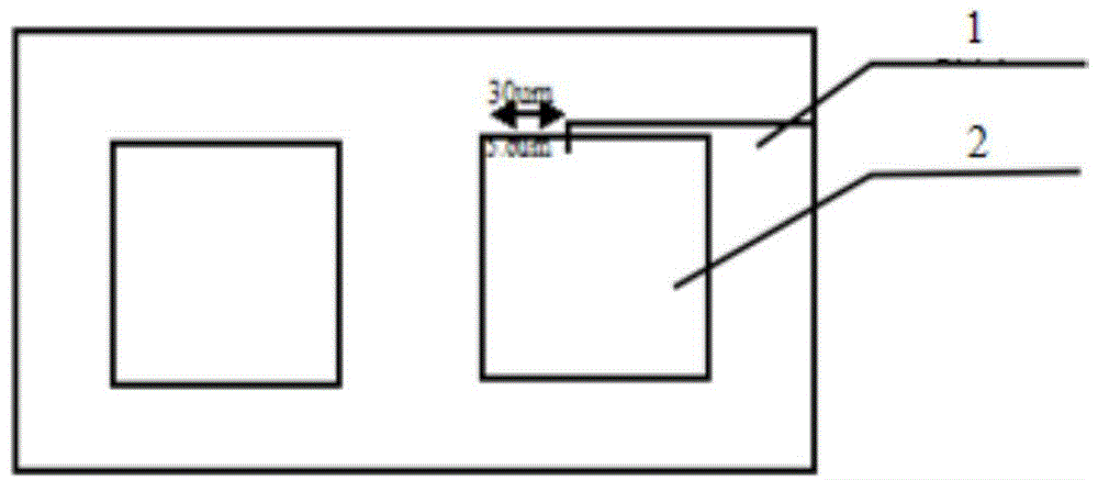
[0033] The present invention is a method for removing solder joints, which is applied to chips containing and testing structures. The solder joints are located on the upper layer of the test structures and partially or completely block the test structures. The method mainly includes the following steps:

[0034] Step S1, removing the metal wire connected to a welding pad through the welding spot;

[0035] Step S2, fixing the chip with the metal wire removed on the sample stage of a probe station;

[0036] Step S3, using the tip of the probe to push the root of the solder joint to completely separate the solder joint from the s...


PUM


Abstract

The invention discloses a method for removing welding spots. The method comprises the steps that firstly, a metal line connected to a welding pad through the welding spots is removed; secondly, a chip with the metal line removed is fixed to a sample platform of a probe station; thirdly, the probe tip of a probe is used for pushing the root of the welding spots so as to disengage the welding spots from the welding pad completely; lastly, the disengaged welding spots are removed from the chip. According to the method, a manual grinding method is not adopted, the welding pad and a to-be-analyzed structure cannot be abraded, physical positioning and following analyzing are not affected, and the success rate of manufactured samples is increased; the welding spots are removed through the probe, the chip cannot be contaminated, the operation process is safe and simple, and the sample manufacturing time is shortened; the old probe in the sample platform of the probe station serves as a tool, cost is hardly produced, and secondary using of the waste resource is achieved.

Description

technical field [0001] The invention relates to the field of semiconductor manufacturing, in particular to a method for removing solder joints. Background technique [0002] In the semiconductor manufacturing process, it is necessary to perform failure analysis on the chip. Due to the operation of technicians and other problems, the solder joints of the metal leads often exceed the chip pads, and cover the structure of the lower layer of the chip to be analyzed, so that the follow-up analysis The physical location of the is affected (eg figure 1 with figure 2 shown); if the OBRICH mode of the Emission Microscope (EMMI) is used to locate the abnormal point on the chip, if the abnormal point is just in the lower layer blocked by the solder joint, then the photon or laser signal will be soldered The point is blocked, so that the correct positioning result cannot be obtained. [0003] Focused Ion Beam (FIB for short) is used to make cross-sectional faults at the structure, w...

Claims


Application Information

Patent Timeline
Patent Type & Authority Applications(China)
IPC IPC(8): H01L21/60B23K1/018
CPCH01L2224/05554H01L24/98B23K1/018H01L2224/98
Inventor 白月
Owner SHANGHAI HUALI MICROELECTRONICS CORP
Why Eureka
Try Eureka