Manufacturing method of array substrate, array substrate and display device

A technology of an array substrate and a manufacturing method, which is applied in the field of manufacturing array substrates, can solve the problems of insufficient charging of thin film transistors, increased parasitic capacitance, problems with images of display devices, etc., so as to enhance the anti-static breakdown and leakage capabilities, and reduce parasitics. Capacitance, improving electrical properties and the effect of storage capacitors

Active Publication Date: 2017-08-11
BOE TECH GRP CO LTD
View PDF7 Cites 0 Cited by
  • Summary
  • Abstract
  • Description
  • Claims
  • Application Information

AI Technical Summary

Problems solved by technology

When simply selecting a gate insulating material with a low dielectric constant or increasing the thickness of the gate insulating layer to reduce the parasitic capacitance to improve the response speed, the characteristics and storage capacitance of the thin film transistor will be reduced at the same time, resulting in insufficient charging of the thin film transistor on the array substrate. which in turn causes problems with the image on the display
Conversely, if the electrical characteristics and storage capacitance of thin film transistors are improved simply by using an ultra-thin gate insulating layer or increasing the dielectric constant of the gate insulating layer, it will also lead to an increase in parasitic capacitance, which will lead to leakage of the array substrate, life and reliability. Sexual variation and other issues

Method used


Image

  • Manufacturing method of array substrate, array substrate and display device
  • Manufacturing method of array substrate, array substrate and display device
  • Manufacturing method of array substrate, array substrate and display device

Examples


Embodiment Construction

[0038] The following will clearly and completely describe the technical solutions in the embodiments of the present invention with reference to the accompanying drawings in the embodiments of the present invention. Obviously, the described embodiments are only some, not all, embodiments of the present invention. Based on the embodiments of the present invention, all other embodiments obtained by persons of ordinary skill in the art without making creative efforts belong to the protection scope of the present invention.

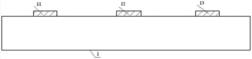
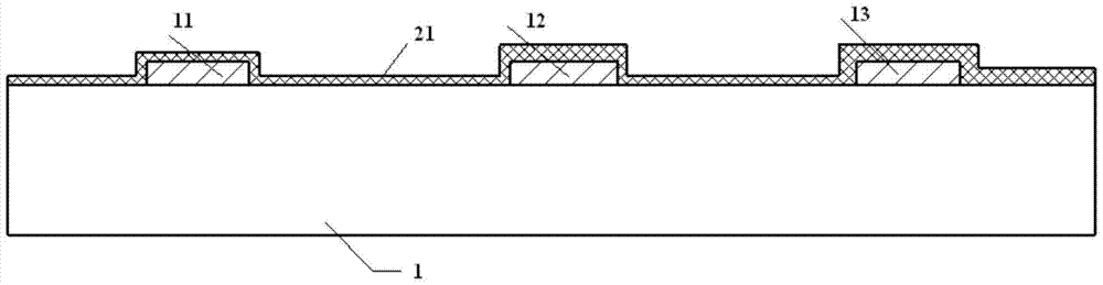
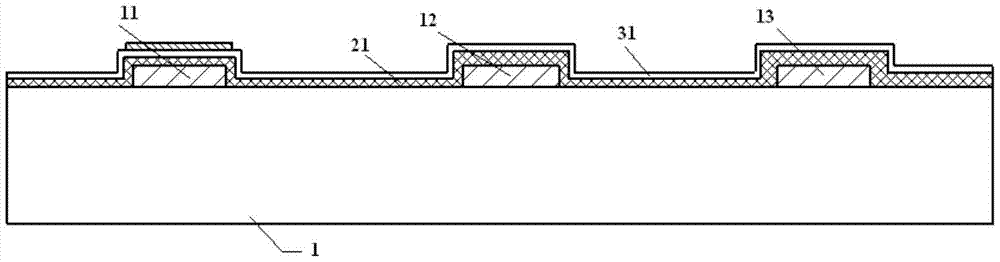
[0039] The method for manufacturing an array substrate according to an embodiment of the present invention includes the steps of providing a gate metal layer and a source-drain metal layer on the substrate, the gate metal layer including the gate of the thin film transistor and the first electrode of the storage capacitor plate, the source and drain metal layer includes the source of the thin film transistor, the drain of the thin film transistor and the second...


PUM


Abstract

The invention provides a manufacturing method of an array substrate, an array substrate and a display device. The manufacturing method of the array substrate includes the step of arranging a grid metal layer on the substrate and the step of arranging a source drain metal layer on the substrate, the grid metal layer comprises a grid electrode of a thin film transistor and a first pole plate of a storage capacitor, and the source drain metal layer comprises a source electrode and a drain electrode of the thin film transistor and a second pole plate of the storage capacitor; between the step of arranging the grid metal layer and the step of arranging the source drain metal layer, the manufacturing method of the array substrate further includes the steps that at least one non-channel contact interface grid insulating layer is arranged on the substrate, the part, corresponding to the grid electrode and / or the first pole plate, of the non-channel contact interface grid insulating layer is graphed and wholly or partially thinned; a channel contact interface grid insulating layer which is not graphed is arranged on the substrate, and a channel layer of the thin film transistor is arranged on the channel contact interface grid insulating layer. The electrical properties and the storage capacitance of the thin film transistor are improved, and stray capacitance is reduced.

Description

technical field [0001] The present invention relates to the technical field of manufacturing an array substrate, in particular to a method for manufacturing an array substrate, an array substrate and a display device. Background technique [0002] In the existing manufacturing process of the array substrate, the gate insulating layer is simultaneously the dielectric layer of the thin film transistor and the dielectric layer of the storage capacitor. When simply selecting a gate insulating material with a low dielectric constant or increasing the thickness of the gate insulating layer to reduce the parasitic capacitance to improve the response speed, the characteristics and storage capacitance of the thin film transistor will be reduced at the same time, resulting in insufficient charging of the thin film transistor on the array substrate. This then leads to problems with the image of the display device. Conversely, if the electrical characteristics and storage capacitance o...

Claims


Application Information

Patent Timeline
Patent Type & Authority Patents(China)
IPC IPC(8): H01L21/82H01L21/28H01L21/336H01L29/423H01L29/786H01L27/02
CPCH01L21/28H01L21/77H01L27/12H01L29/42364H01L29/42384
Inventor 刘晓娣盖翠丽孙力王刚
Owner BOE TECH GRP CO LTD
Why Eureka
Try Eureka