Array substrate and display device
An array substrate, pixel unit technology, applied in optics, instruments, electrical components, etc., can solve the problems affecting the aperture ratio of pixel units, the influence of aperture ratio, etc., and achieve the effect of reducing the area, increasing the aperture ratio, and improving the aperture ratio.
- Summary
- Abstract
- Description
- Claims
- Application Information
AI Technical Summary
Problems solved by technology
Method used
Image

Examples
Embodiment 1
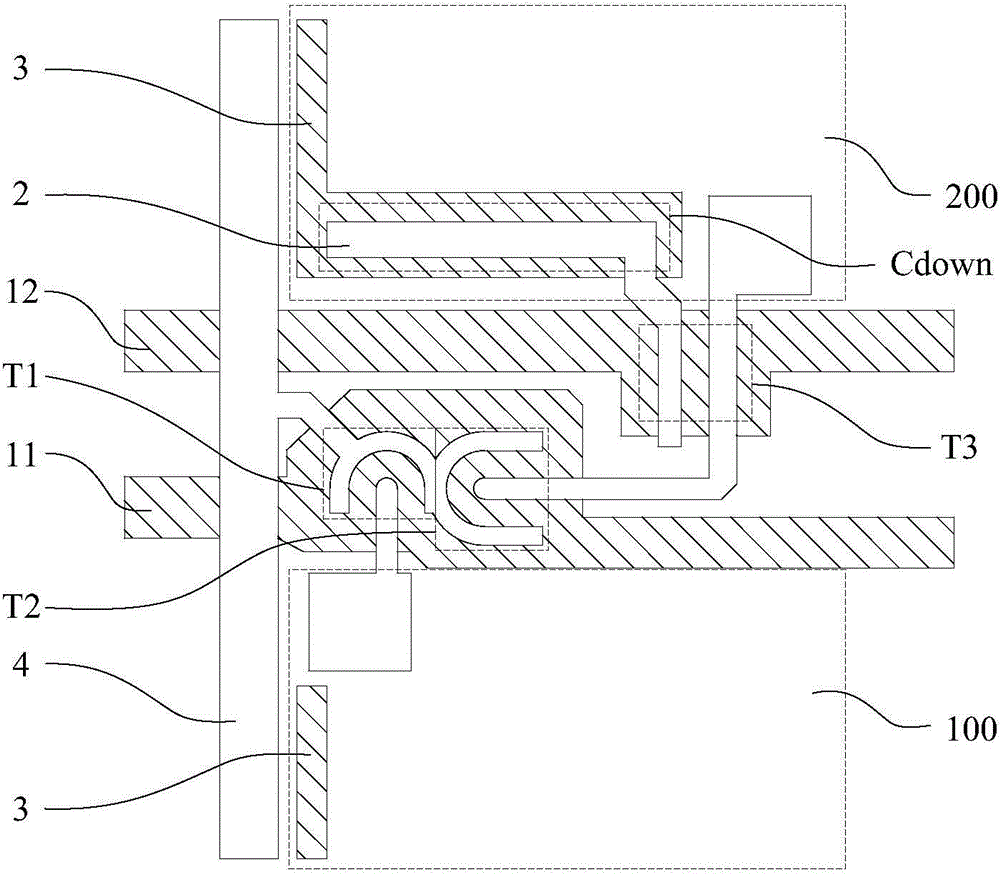
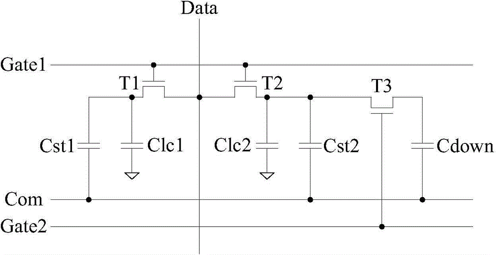
[0035] An embodiment of the present invention provides an array substrate, which can be applied to a VA-type liquid crystal display, and the array substrate includes several pixel units. Such as image 3 and Figure 4 As shown, the pixel unit includes a main pixel area 100 , a sub-pixel area 200 , a first voltage dividing capacitor Cdown1 , a driving scanning line ( Gate1 ) 11 and a voltage dividing scanning line ( Gate2 ) 12 . The main pixel area 100 is provided with a main pixel electrode (not shown in the figure), and the sub-pixel area 200 is provided with a sub-pixel electrode (not shown in the figure).
[0036] In this embodiment, the first voltage-dividing capacitor is formed by overlapping the voltage-dividing electrode 2 and the driving scanning line 11 . During the display process, the driving scanning lines 11 of each row of pixel units are scanned row by row, so at any moment, only one driving scanning line 11 is at a high potential, and the time for any one driv...
Embodiment 2
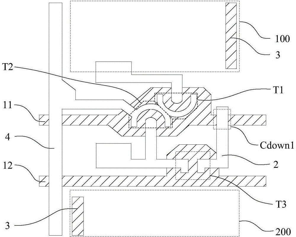
[0047] An embodiment of the present invention provides an array substrate, which can be applied to a VA-type liquid crystal display, and the array substrate includes several pixel units. Such as Figure 7 and Figure 8 As shown, the pixel unit includes a main pixel area 100 , a sub-pixel area 200 , a first voltage dividing capacitor Cdown1 , a driving scanning line ( Gate1 ) 11 and a voltage dividing scanning line ( Gate2 ) 12 . The main pixel area 100 is provided with a main pixel electrode (not shown in the figure), and the sub-pixel area 200 is provided with a sub-pixel electrode (not shown in the figure).
[0048] In this embodiment, the first voltage-dividing capacitor is formed by overlapping the voltage-dividing electrode 2 and the voltage-dividing scanning line 12 . During the display process, the voltage-divided scanning lines 12 of each row of pixel units are scanned row by row, so at any moment, only one voltage-divided scanning line 12 is at a high potential, and...
Embodiment 3
[0059] An embodiment of the present invention provides a display device, preferably a VA display device, specifically, a liquid crystal television, a liquid crystal display, a mobile phone, a tablet computer, and the like. The display device includes a color filter substrate and the array substrate provided by the above-mentioned embodiments of the present invention.
PUM
 Abstract
Description
Claims
Application Information
 - Generate Ideas
- Intellectual Property
- Life Sciences
- Materials
- Tech Scout
- Unparalleled Data Quality
- Higher Quality Content
- 60% Fewer Hallucinations
Browse by: Latest US Patents, China's latest patents, Technical Efficacy Thesaurus, Application Domain, Technology Topic, Popular Technical Reports.
© 2025 PatSnap. All rights reserved.Legal|Privacy policy|Modern Slavery Act Transparency Statement|Sitemap|About US| Contact US: help@patsnap.com