Photoelectronic imaging system optical axis difference rapid detection method and device

A photoelectric imaging and imaging system technology, which is applied in the direction of measuring devices, optical devices, instruments, etc., can solve the problems of low precision, poor environmental adaptability, and limitations, and achieve improved accuracy and efficiency, high repeatability, and fast correction speed Effect

Active Publication Date: 2015-04-08
NAT UNIV OF DEFENSE TECH
View PDF6 Cites 8 Cited by
  • Summary
  • Abstract
  • Description
  • Claims
  • Application Information

AI Technical Summary

Problems solved by technology

Calibration with this method usually takes several times to calibrate, the calibration process is cumbersome, the accuracy is poor, and the efficiency is low
[0006] (2) Laser red dot type calibration mirror: The calibration device emits laser light, and the crosshairs of the photoelectric equipment are manually adjusted to coincide with the red dot, and the calibration is completed, but the energy of the laser red dot is small, and the use conditions are limited. It is difficult to distinguish tens of meters away, and can only be used at dawn, dusk, and cloudy days, and the calibration device actively emits laser light, which is limited in many practical applications
This calibration method requires the use of complex instruments and equipment, the calibration process is cumbersome and slow, and the calibration accuracy can generally reach within 1MOA
[0008] In summary, in view of the existing calibration devices generally have many defects such as cumbersome calibration process, slow speed, low accuracy, poor repeatability, and poor environmental adaptability, there is an urgent need for a high-precision calibration device that can take into account both calibration accuracy and calibration efficiency accuracy. Quick Calibration

Method used


Image

  • Photoelectronic imaging system optical axis difference rapid detection method and device
  • Photoelectronic imaging system optical axis difference rapid detection method and device
  • Photoelectronic imaging system optical axis difference rapid detection method and device

Examples


Embodiment Construction

[0034] The present invention will be further described in detail below in conjunction with the accompanying drawings and specific embodiments.

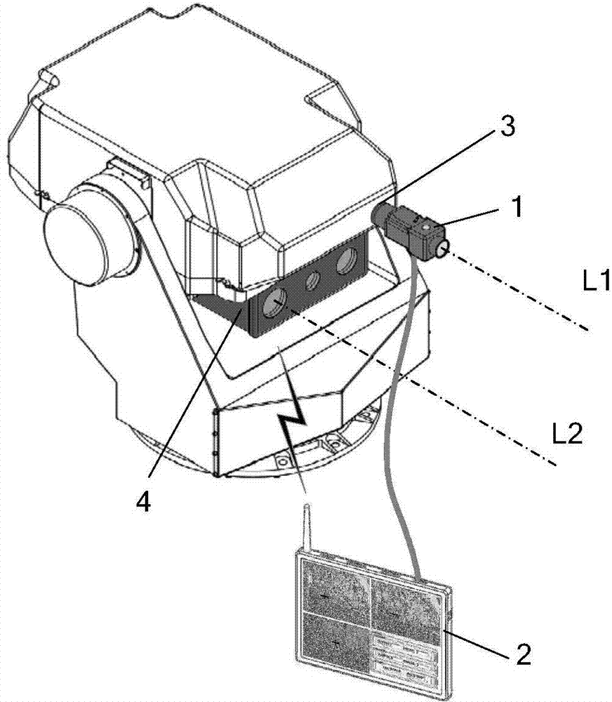
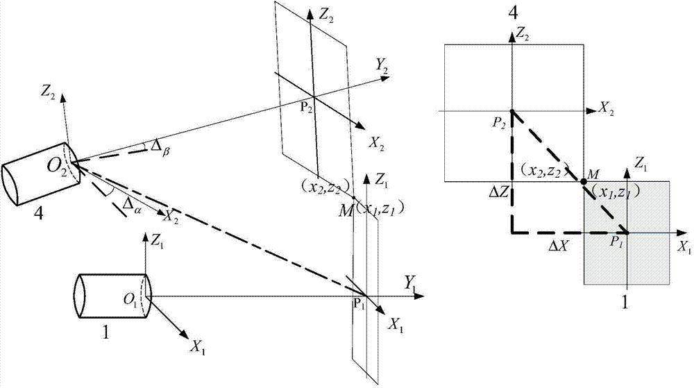
[0035] Such as figure 2As shown, the photoelectric imaging system optical axis deviation rapid detection method of the present invention is to use the photoelectric imaging system 4 under test and the reference imaging system (rapid detection device), take image metrology as the basic principle, and use the Sobel edge extraction algorithm to extract the reference imaging The image contour edge of the system and the photoelectric imaging system 4 under test is integrated and binarized to obtain the contour edge feature image, and any feature-obvious target point M in the image of the reference imaging system (correction reference mirror 1) is selected as a reference, and the target The coordinates of point M in the image of the reference imaging system (correction reference mirror 1) are (x1, z1). Search in and determine that the con...


PUM


Abstract

The invention discloses a photoelectronic imaging system optical axis difference rapid detection method and device. The method comprises the steps that a tested photoelectronic imaging system and a standard imaging system are used for acquiring images at the same time, any obvious feature target in the standard imaging system serves as the standard, a target image contour edge extraction and feature matching method is used for analyzing the difference of the same obvious feature target in the tested photoelectronic imaging system and the standard imaging system, and the difference of the aiming light of the tested photoelectronic imaging system is obtained. The device is used for implementing the method. The photoelectronic imaging system optical axis difference rapid detection method and device have the advantages that the principle is simple, operation is convenient, calibration accuracy is high, and calibration efficiency is high.

Description

technical field [0001] The invention mainly relates to the technical field of photoelectric imaging, in particular to a method and device for quickly detecting optical axis deviation among multiple photoelectric imaging systems. Background technique [0002] With the development of optoelectronic technology, electrical sensor systems such as laser rangefinders, laser-guided irradiation, visible light imaging, and infrared imaging have been widely used in optoelectronic image detection equipment in the fields of surveying and mapping, surveillance, early warning, guidance, remote sensing, and disaster relief. application. Among many applications, "optical axis pointing accuracy" has become an important parameter to measure the performance of multi-optical axis photoelectric equipment. The misalignment of the system also requires timely calibration of the optical axis during use. [0003] At present, the optical axis deviation detection equipment is difficult to adapt to the...

Claims


Application Information

Patent Timeline
Patent Type & Authority Applications(China)
IPC IPC(8): G01B11/27
Inventor 刘华黄征宇张连超陈宁魏维范世珣范大鹏
Owner NAT UNIV OF DEFENSE TECH
Why Eureka
Try Eureka