A self-extinguishing self-recovery avalanche photodiode

An avalanche photoelectric and self-recovery technology, applied in circuits, electrical components, semiconductor devices, etc., can solve the problems of high cost and complicated extinguishing circuit system

Active Publication Date: 2017-04-05
BEIJING UNIV OF TECH
View PDF6 Cites 0 Cited by
  • Summary
  • Abstract
  • Description
  • Claims
  • Application Information

AI Technical Summary

Problems solved by technology

The increase of extinguishing circuit makes the whole system complex and costly

Method used


Image

  • A self-extinguishing self-recovery avalanche photodiode
  • A self-extinguishing self-recovery avalanche photodiode
  • A self-extinguishing self-recovery avalanche photodiode

Examples


Embodiment Construction

[0027] As shown in Figure 5, its preparation process and method are as follows:

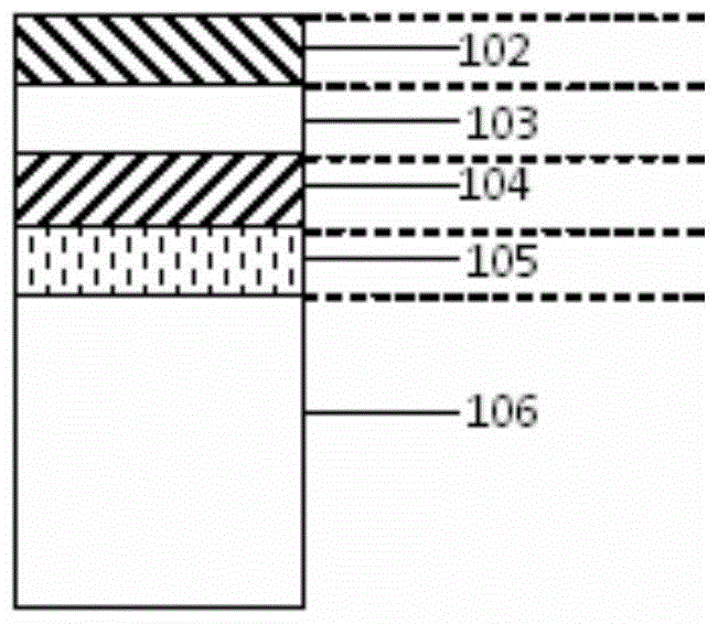
[0028] 1. Phosphorus is implanted on the front surface of a high-resistance silicon substrate with a resistivity of 1000Ω·cm or more to form a hole potential well formation layer 105 with a doping concentration of 1×10 18 cm -3 ;

[0029] 2. Implant boron on the front side of the high-resistance silicon substrate to form a p-type layer 104 with a doping concentration of 5×10 17 cm -3 ;

[0030] 3. Phosphorus is implanted into the front side of the silicon substrate, and an n-type layer 102 is formed on the upper surface of the sample, with a doping concentration of 5×10 18 cm -3 . At the same time, due to the difference in implantation depth between the n-type layer 102 and the p-type layer 104 formed by ion implantation, there will be a layer of unintentionally doped region 103 between them, which is a charge multiplication region;

[0031] 4. Annealing, activate the implanted impurity io...


PUM


Abstract

The invention provides a self-extinguishing and self-recovering avalanche photodiode, and relates to the field of semiconductor photoelectric devices. Different from a conventional structure, the avalanche photodiode is characterized by automatic extinguishing and then automatic recovering. The avalanche photodiode comprises an n-type layer (102), a charge multiplication region (103), a p-type layer (104), and a substrate (106) stacked longitudinally in sequence. The avalanche photodiode is characterized in that a cavity potential well forming layer (105) is between the p-type layer (104) and the substrate (106). A cavity potential well can be formed by two methods, one is that the cavity potential well forming layer (105) uses an n-type material, when the material and the p-type layer (104) form a pn junction, an energy band moves down, so that cavity position energy of the p-type layer (104) is lowest, so that the cavity potential well is formed in the p-type layer (104). The second method is that the cavity potential well forming layer (105) uses a p+ type material whose doping density is more than two times of that of the p-type layer (104), and after an nn+ junction is formed, a cavity potential well is formed in the cavity potential well forming layer (105).

Description

technical field [0001] The invention relates to the field of semiconductor optoelectronic devices, in particular to an avalanche photodiode capable of detecting weak light. Background technique [0002] Single-photon detection technology has broad application prospects in quantum communication, sensing and remote sensing, high-energy physics, 3D imaging, military and medicine, so it has attracted much attention. At present, photon counter devices for single photon detection are mainly divided into two structures: photomultiplier tube PMT (Photomultiplier tube) based on vacuum tube technology and avalanche photon diode (Avalanche Photon Diode, APD) based on semiconductor technology. The photomultiplier tube has the advantages of high gain, large test area, fast calculation rate, and high time resolution. However, its quantum efficiency in the visible light range is very low, the volume is large, it is difficult to integrate, it works at high voltage (200-600V), and it is easy...

Claims


Application Information

Patent Timeline
IPC IPC(8): H01L31/107
CPCH01L31/107
Inventor 郭霞李冲刘巧莉董建刘白
Owner BEIJING UNIV OF TECH
Why Eureka
Try Eureka