Semiconductor Wafer Handling Equipment

A semiconductor and wafer technology, applied in the field of semiconductor wafer conveying equipment, can solve the problems of poor energy efficiency, excess cost, defects, etc., and achieve the effects of preventing power consumption, reducing work burden, and suppressing defective products

Active Publication Date: 2016-08-17
SENJU METAL IND CO LTD
View PDF6 Cites 0 Cited by
  • Summary
  • Abstract
  • Description
  • Claims
  • Application Information

AI Technical Summary

Problems solved by technology

As a result, the energy efficiency deteriorates, and as a result of heating to bring the low-temperature portion to the necessary temperature, the overheated portion other than the low-temperature portion is damaged, causing unnecessary costs and defects.

Method used


Image

  • Semiconductor Wafer Handling Equipment
  • Semiconductor Wafer Handling Equipment
  • Semiconductor Wafer Handling Equipment

Examples


Embodiment Construction

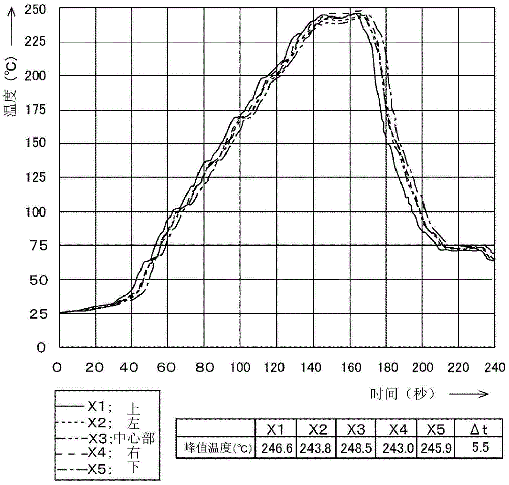
[0030] An object of the present invention is to provide a semiconductor wafer transfer tool capable of uniformly heating the surface of the wafer when heating the semiconductor wafer.

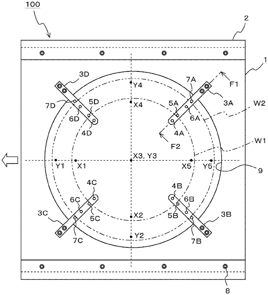
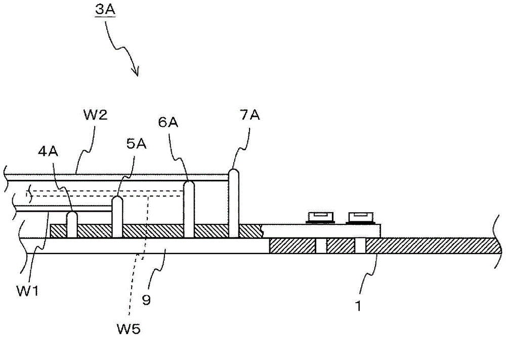
[0031] Next, embodiments of the present invention will be described with reference to the drawings. figure 1 is a plan view of an embodiment of the semiconductor wafer transfer tool of the present invention, figure 2 Shows examples of shapes of holding pins and wafer misalignment prevention guides (hereinafter simply referred to as prevention guides), figure 1 The enlarged view of the F1-F2 direction of the section.

[0032] That is, the wafer transport tool 100 of the embodiment constitutes an example of a semiconductor wafer transport tool, and is a tool for holding and transporting a semiconductor wafer in a semiconductor manufacturing process. There is an opening 9 at the center of the bottom plate 1 serving as an example of the main body, and conveying guides 2 are attached to the lef...


PUM


Abstract

The semiconductor wafer conveying tool which can realize the uniform heating to a surface of a semiconductor wafer when heating the semiconductor wafer is a semiconductor wafer conveying tool which holds the semiconductor wafer having a predetermined diameter to convey it wherein the tool is provided with a main body having an opening with a diameter which is larger than a diameter of the semiconductor wafer, and at least three supporting members each having a predetermined length, containing plural pins which are arranged corresponding to the diameter of the semiconductor wafer and being configured to be a holding mechanism for holding the semiconductor wafer concentrically at a projection position from an inner periphery portion of the main body around the opening, as shown in FIG. 1 .

Description

technical field [0001] The present invention relates to a transport tool for transporting semiconductor wafers in a semiconductor manufacturing process, and particularly relates to a semiconductor wafer transport tool capable of uniformly heating a semiconductor wafer during heating. Background technique [0002] Conventionally, in a semiconductor wafer heat treatment process and a transport line in a semiconductor manufacturing process, in order to transfer and transport a large number of semiconductor wafers, dedicated transport tools have been used. [0003] The size of the semiconductor wafer to be transported may vary from wafer to wafer. Therefore, in order to omit the process of replacing the transfer tool every time the size of the transfer object changes, a transfer tool capable of handling wafers of multiple sizes with a single transfer tool is known (see Patent Document 1 and Patent Document 2). [0004] In Patent Document 1, there is disclosed a wafer fork (Japa...

Claims


Application Information

Patent Timeline
Patent Type & Authority Patents(China)
IPC IPC(8): H01L21/673B65G49/07
CPCH01L21/6875H01L21/67346H01L21/68707
Inventor 六辻利彦长田要
Owner SENJU METAL IND CO LTD
Why Eureka
Try Eureka