3D imaging optical radar system based on LED light source

A technology of LED light source and light radar, applied in radio wave measurement system, electromagnetic wave re-radiation, utilization of re-radiation, etc., can solve the problem of difficulty in cost reduction, and achieve the effect of cost reduction and low cost

Inactive Publication Date: 2015-04-22
UNIV OF ELECTRONIC SCI & TECH OF CHINA
View PDF7 Cites 2 Cited by
  • Summary
  • Abstract
  • Description
  • Claims
  • Application Information

AI Technical Summary

Problems solved by technology

In any case, due to the need for echo modulation (actually gain modulation), expensive ICCD devices are required. The former requires a laser with high power and high modulation rate, and the latter also uses a pulsed laser. These Factors have directly led to the difficulty in reducing its cost
In addition, these schemes using 2D sensors to realize 3D imaging are basically still in the stage of theoretical and experimental research, and there is still a certain distance from engineering testing, and there are still many theoretical and technical problems to be solved

Method used


Image

  • 3D imaging optical radar system based on LED light source
  • 3D imaging optical radar system based on LED light source
  • 3D imaging optical radar system based on LED light source

Examples


Embodiment Construction

[0014] The present invention will be further described below in conjunction with the examples.

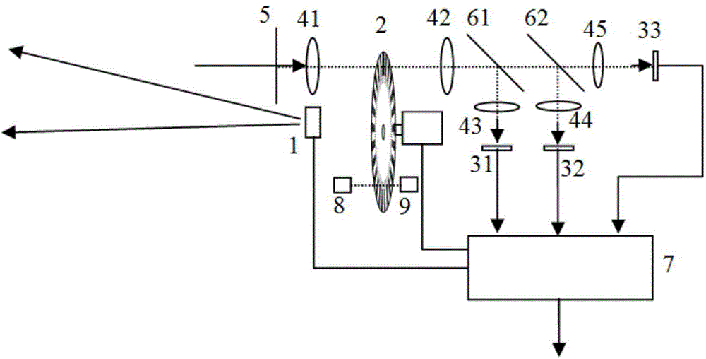
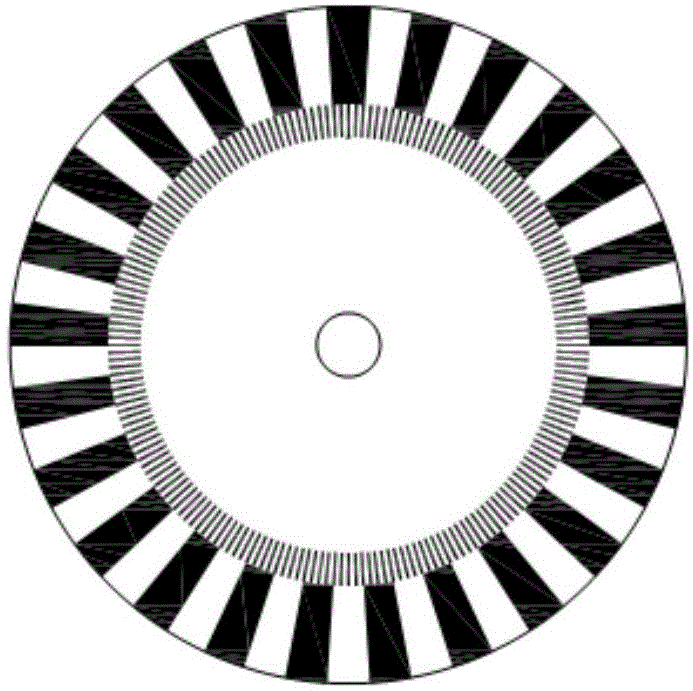
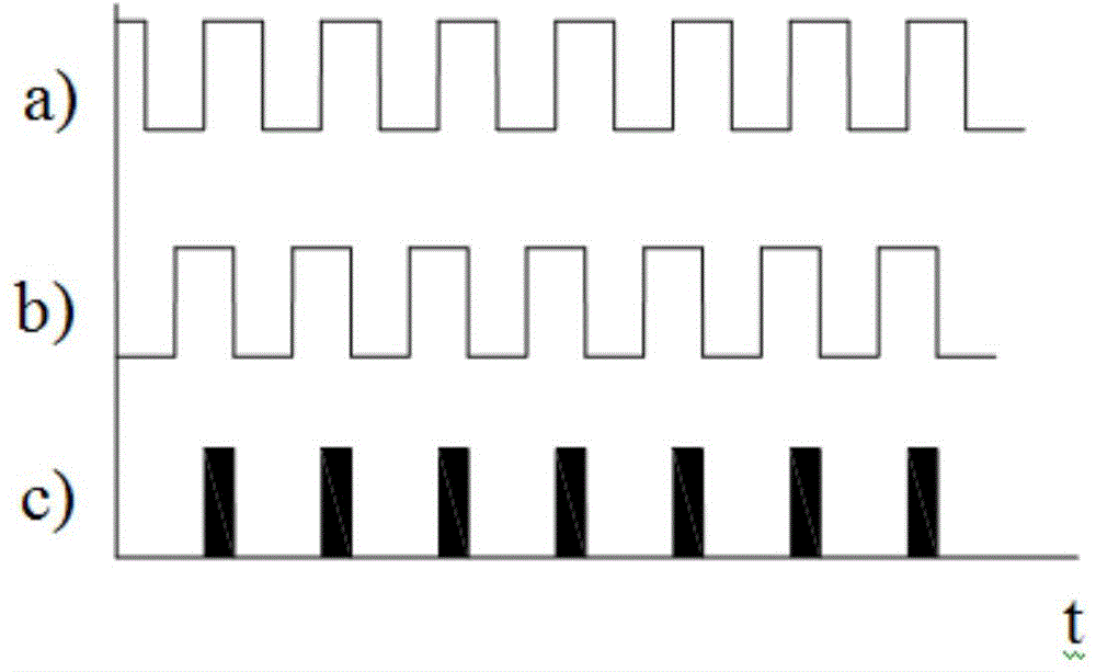
[0015] Such as figure 1 As shown, it is a schematic diagram of the principle of 3D imaging lidar based on LED illumination.

[0016] High-power and high-speed LED light emitting components can be welded on the same PCB board with multiple packaged light-concentrating high-speed in-line LEDs, and the corresponding drive circuit is configured on the PCB board, and one drive circuit can be used to drive multiple serial connections at the same time. LEDs are combined in multiple ways to construct an LED light emitting component with a certain field of view. For example, 10 one-way drivers are used to combine 10 channels to construct 100 LED lights to illuminate a field of view at the same time. If the peak power of each light is 150mW, the total peak power can reach 15W, and the space interval between LED lights is 6mm. Then only a space position of 60mm×60mm is needed. More LED com...


PUM


Abstract

The invention provides a 3D imaging optical radar system based on an LED light source. The 3D imaging optical radar system is used for reducing cost of an existing 3D imaging optical radar system. The 3D imaging optical radar system comprises a high-power high-speed LED light emitting assembly, a high-speed rotating modulation disc, a first optical imaging lens, a second optical imaging lens, three imaging assemblies, a light filter, a light splitter and a data processing module. Echo light beams reflected by a target reach the first optical imaging lens after passing through the light filter to be imaged on the high-speed rotating modulation disc, modulated light waves then enter the second optical imaging lens, and light outputted by the second optical imaging lens passes through the light splitter and then enters the three imaging assemblies; each imaging assembly comprises an optical imaging lens and a single-color CCD sensor, wherein light reaches the single-color CCD sensor after passing through the optical imaging lens, and the output end of the single-color CCD sensor is connected with the data processing module. Through a reasonable 3D imaging mechanism, high-power high-speed LEDs low in cost and the CCD sensors low in cost are adopted, and therefore cost is greatly reduced.

Description

technical field [0001] The present invention relates to imaging light radar technology, mainly relates to the light radar technology using 2D sensor to realize 3D imaging, specifically a 3D imaging light radar system based on LED light source. Background technique [0002] Optical imaging radar (Lidar) basically uses laser as the emission light source, which is inseparable from the characteristics of laser. Imaging lidar can acquire 3D images of targets and has important application value. Scanless imaging is a research hotspot in recent years, and it is mainly developing in two directions. One direction is to develop 3D sensors, and the other direction is to use 2D sensors to realize 3D imaging. The most representative of the former is the FLASH radar developed by Lincoln Laboratory. Its focus is to develop a FLASH device with a three-dimensional imaging function. This device is a two-dimensional pixel array device, and each pixel has an independent ranging function. The F...

Claims


Application Information

Patent Timeline
IPC IPC(8): G01S17/89
CPCG01S7/481G01S17/89
Inventor 彭仁军夏丽娜徐振华
Owner UNIV OF ELECTRONIC SCI & TECH OF CHINA
Why Eureka
Try Eureka