Check patentability & draft patents in minutes with Patsnap Eureka AI!

OLED display device and manufacturing method thereof

A technology for display devices and manufacturing methods, which is applied in the manufacture of semiconductor/solid-state devices, electric solid-state devices, semiconductor devices, etc., can solve problems such as leakage of emitted light, and achieve the effects of reducing interface problems, improving display quality, and reducing short-circuit defects.

Active Publication Date: 2017-10-13
TCL CHINA STAR OPTOELECTRONICS TECH CO LTD
View PDF4 Cites 0 Cited by
  • Summary
  • Abstract
  • Description
  • Claims
  • Application Information

AI Technical Summary

Problems solved by technology

However, due to increasing user demands for low-power / high-resolution products, it is necessary to solve the problem of leaking emitted light without reducing the efficiency of light-emitting materials or reducing the resolution of display devices.

Method used


Image

  • OLED display device and manufacturing method thereof
  • OLED display device and manufacturing method thereof

Examples


Embodiment Construction

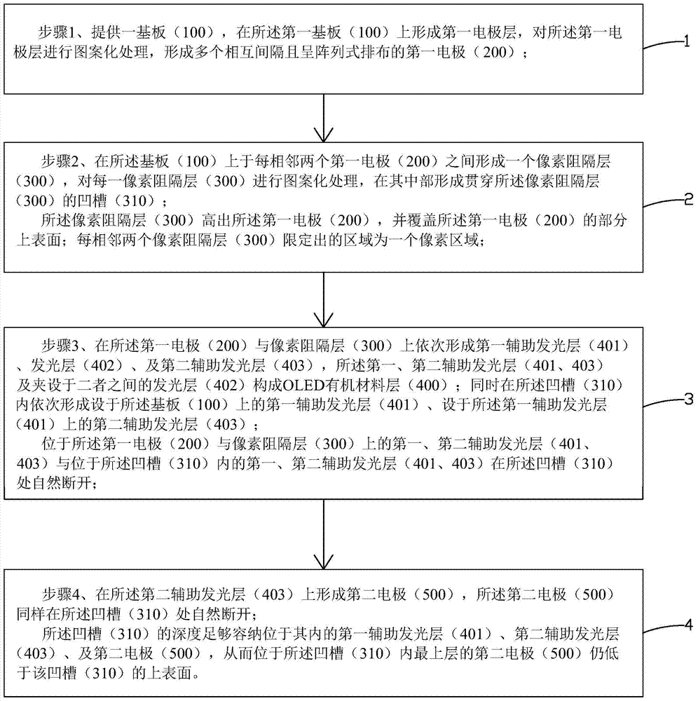
[0038] In order to further illustrate the technical means adopted by the present invention and its effects, the following describes in detail in conjunction with preferred embodiments of the present invention and accompanying drawings.

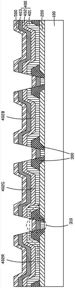
[0039] see figure 1 , the present invention firstly provides an OLED display device, comprising:

[0040] Substrate 100;

[0041] A plurality of first electrodes 200 spaced from each other and arranged in an array on the substrate 100;

[0042] A pixel barrier layer 300 disposed on the substrate 100 and located between every two adjacent first electrodes 200; the pixel barrier layer 300 is higher than the first electrode 200 and covers the first electrode 200 Part of the upper surface; each pixel barrier layer 300 has a groove 310 in the middle, and the groove 310 runs through the pixel barrier layer 300; the area defined by every two adjacent pixel barrier layers 300 is a pixel area;

[0043]The OLED organic material layer 400 disposed on ...


PUM


Abstract

The invention provides an OLED display device and a manufacturing method thereof. The OLED display device comprises: a substrate (100); a plurality of first electrodes (200) spaced apart from each other and arranged in an array on the substrate (100); A pixel barrier layer (300) between the two first electrodes (200); each pixel barrier layer (300) has a groove (310) in the middle, and the groove (310) runs through the pixel barrier layer (300) the OLED organic material layer (400) disposed on the first electrode (200) and the pixel barrier layer (300); the OLED organic material layer (400) is disconnected at the groove (310); and The second electrode (500) arranged on the OLED organic material layer (400); the second electrode (500) is also disconnected at the groove (310). The OLED display device can suppress the leaked emitted light caused by leakage current, reduce short-circuit defects, improve the reliability of the OLED display device, and improve the display quality of the OLED display device.

Description

technical field [0001] The invention relates to the field of display technology, in particular to an OLED display device and a manufacturing method thereof. Background technique [0002] In recent years, flat panel displays such as Liquid Crystal Display (LCD) and Organic Light Emitting Diode (OLED) displays have gradually replaced CRT displays and become mainstream products in the display market. Among them, OLED displays have many advantages such as self-illumination, low driving voltage, high luminous efficiency, short response time, high definition and contrast, nearly 180° viewing angle, wide operating temperature range, flexible display and large-area full-color display, etc. It is recognized by the industry as the display with the most development potential. [0003] OLED display devices generally include: a substrate, an anode disposed on the substrate, a hole injection layer disposed on the anode, a hole transport layer disposed on the hole injection layer, a light...

Claims


Application Information

Patent Timeline
Patent Type & Authority Patents(China)
IPC IPC(8): H01L27/32H01L21/77
CPCH10K59/805
Inventor 李文辉王宜凡
Owner TCL CHINA STAR OPTOELECTRONICS TECH CO LTD
Features
  • R&D
  • Intellectual Property
  • Life Sciences
  • Materials
  • Tech Scout
  • Unparalleled Data Quality
  • Higher Quality Content
  • 60% Fewer Hallucinations
Learn More