Check patentability & draft patents in minutes with Patsnap Eureka AI!

Processing device

A technology for processing devices and objects to be processed, which can be applied to fine working devices, stone processing equipment, metal processing equipment, etc., and can solve the problem of inability to detect the volume of debris in the cross-sectional shape of the processing groove.

Active Publication Date: 2018-02-16
DISCO CORP
View PDF6 Cites 0 Cited by
  • Summary
  • Abstract
  • Description
  • Claims
  • Application Information

AI Technical Summary

Problems solved by technology

[0009] However, the image captured by the imaging device equipped with a microscope and a camera is a two-dimensional image, and the width or depth of the processing groove formed by cutting or laser processing, and the height or width of the chip can only be roughly measured, and it cannot be measured in the device. Detect the cross-sectional shape of the machining groove and the volume of chips

Method used


Image

  • Processing device
  • Processing device
  • Processing device

Examples


Embodiment Construction

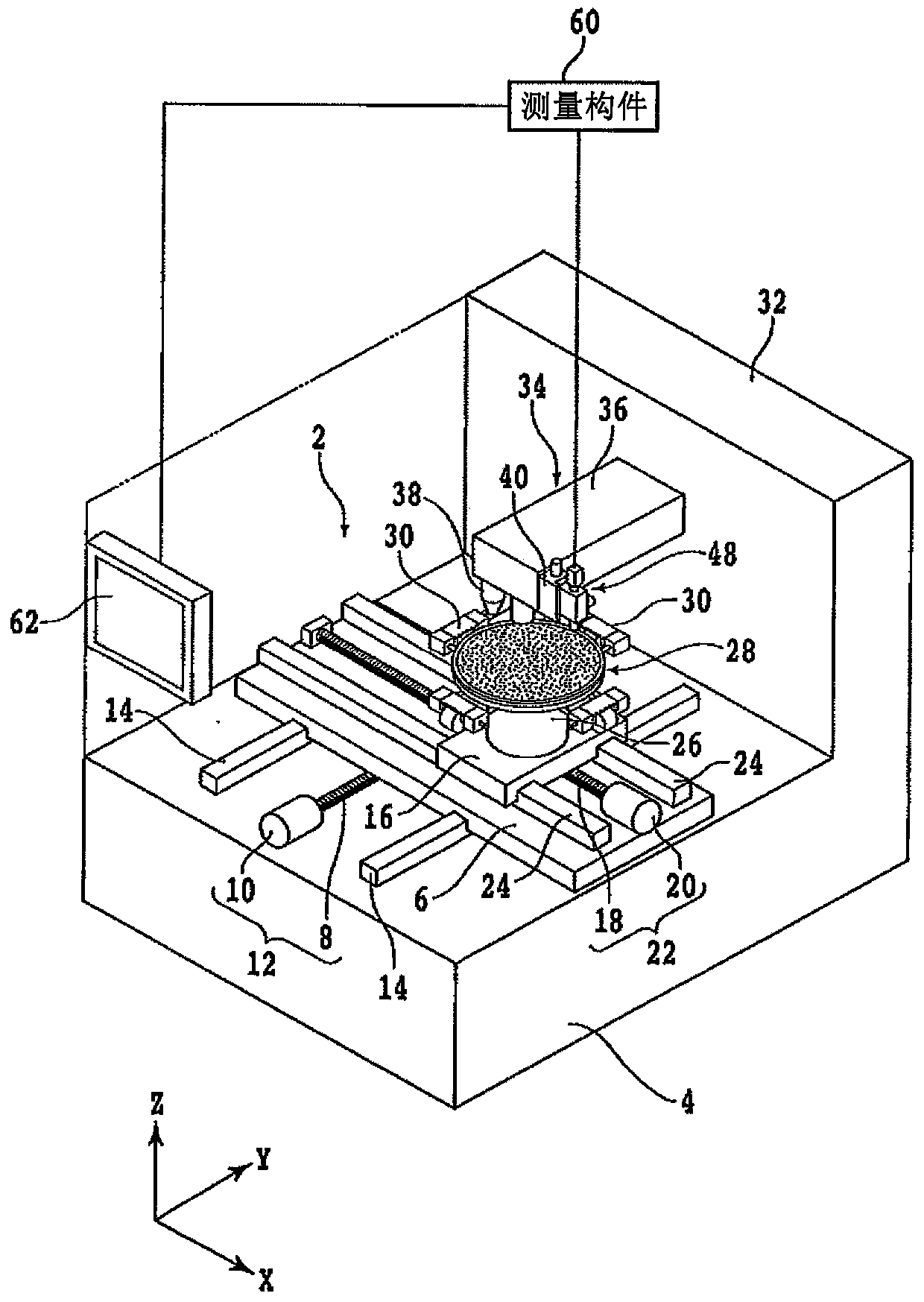
[0063] Hereinafter, embodiments of the present invention will be described in detail with reference to the drawings. refer to figure 1 , is a perspective view showing a laser processing apparatus including the three-dimensional measuring means of the first embodiment. The laser processing device 2 includes a first slider 6 mounted on the stationary base 4 so as to be movable in the Y-axis direction.

[0064] The first slider 6 moves along a pair of guide rails 14 in the indexing direction, that is, the Y-axis direction, via an indexing mechanism 12 composed of a ball screw 8 and a pulse motor 10 .

[0065] The second slider 16 is mounted on the first slider 6 so as to be movable in the X-axis direction. That is, the second slider 16 moves along a pair of guide rails 24 in the machining feed direction, that is, the X-axis direction, via the machining feed mechanism 22 constituted by the ball screw 18 and the pulse motor 20 .

[0066] The chuck table 28 is mounted on the seco...


PUM

PropertyMeasurementUnit
thicknessaaaaaaaaaa

Abstract

The present invention provides a processing device capable of measuring a processing area without taking out a processed object from the processing device. The processing device is provided with a measuring member for measuring the processing area of ​​a workpiece processed by the processing member, and the measuring member is characterized in that the measuring member includes: a three-dimensional measuring member, which is perpendicular to each other in the X-axis direction, the Y-axis direction and the Three-dimensionally measure the workpiece in the Z-axis direction to obtain shape information; and a processing unit that processes the information obtained by the three-dimensional measurement unit and generates image information, the processing unit includes: an image information generation unit that stores the information based on the Z-coordinate The Z coordinate stored in the unit three-dimensionally combines the pixels of the XY coordinates stored in the XY coordinate storage unit to generate image information; and the calculation unit calculates the measurement value of the measurement object of the workpiece based on the generated image information without The processed workpiece can be taken out from the processing device to measure the processing area.

Description

technical field [0001] The present invention relates to processing devices such as laser processing devices and cutting devices. Background technique [0002] Wafers such as silicon wafers and sapphire wafers, which are divided by dividing lines and have IC (Integrated Circuit: Integrated Circuit), LSI (Large Scale Integration: Large Scale Integration) and LEDs formed on the surface, are divided by processing equipment The separated devices are widely used in various electronic devices such as mobile phones and computers. [0003] For dividing wafers, a dicing method using a cutting device called a dicing machine is widely used. In the dicing method, the cutting blade is cut into the wafer while rotating at a high speed of about 30,000 rpm to cut the wafer, and the wafer is divided into individual devices. The cutting blade is fixed with abrasive grains such as diamond by metal or resin. Instead, it is formed to have a thickness of about 30 μm. [0004] On the other hand,...

Claims


Application Information

Patent Timeline
Patent Type & Authority Patents(China)
IPC IPC(8): B28D5/00B28D7/04B28D7/00
CPCB23Q17/20B23Q17/2409B23Q17/2471B23K26/02B23K26/032B23K26/0648B23K26/082
Inventor 伊藤优作大庭龙吾九鬼润一
Owner DISCO CORP
Features
  • R&D
  • Intellectual Property
  • Life Sciences
  • Materials
  • Tech Scout
  • Unparalleled Data Quality
  • Higher Quality Content
  • 60% Fewer Hallucinations
Learn More