

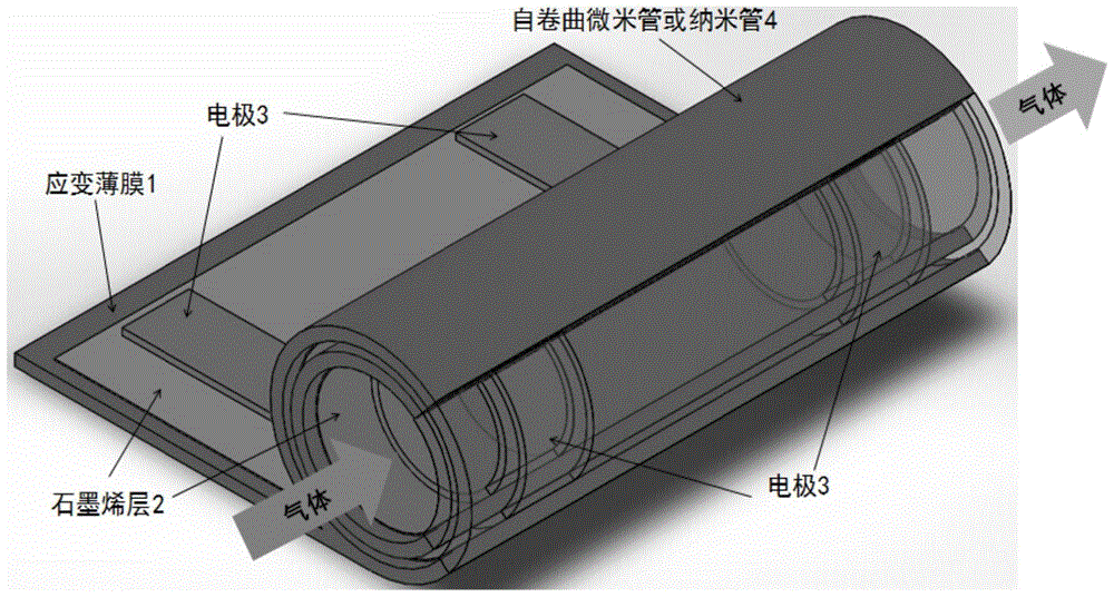
A kind of graphene gas sensor and preparation method thereof
A gas sensor and graphene technology, applied in the sensor field, can solve the problems affecting the stability and reusability of the device, easy to break and pollute, difficult to integrate, etc., to achieve suitable for batch preparation, reduce size, and good repeatability. Effect
- Summary
- Abstract
- Description
- Claims
- Application Information
AI Technical Summary
Problems solved by technology
Method used
Image

Examples
Embodiment 1
[0052] Example 1: Preparation of a graphene gas sensor with III-V group InGaAs / GaAs self-rolling microtubes as a carrier on a Si(100) substrate
[0053] S1: Depositing an AlAs sacrificial layer on a Si substrate;
[0054] After cleaning the Si wafer, put the substrate into the MOCVD reaction chamber; 2 Bake the Si sheet under the atmosphere for 30 minutes, then pass through the AsH 3 Passivate for 30 minutes; cool down to 420°C, grow a low-temperature GaAs nucleation layer with a thickness of 70nm; raise the temperature to 630°C, grow an intermediate temperature GaAs buffer layer with a thickness of 300nm; raise the temperature to 685°C, grow a high-temperature GaAs epitaxial layer with a thickness of 2μm;
[0055] Perform thermal cycle annealing (TCA) on the GaAs epitaxial layer; lower the temperature to 685° C., and grow an AlAs sacrificial layer with a thickness of 50 nm.
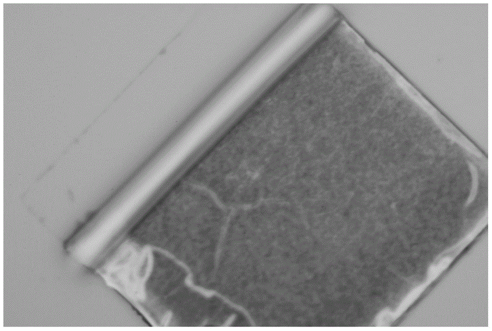
[0056] S2: Depositing an InGaAs / GaAs strained thin film on the AlAs sacrificial layer to obtain a w...
Embodiment 2
[0081] Embodiment 2: Prepare Si / SiO on Si substrate 2 Graphene gas sensor supported by self-curling microtubes
[0082] S1: A 40nm thick Ge sacrificial layer and a 20nm thick Si were successively grown on a Si(100) substrate by using MBE.
[0083] S2: Put it into PECVD and evaporate 25nm thick SiO 2 , with Si / SiO 2 Strained bilayer wafers.
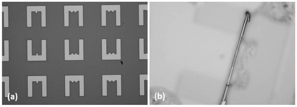
[0084] S3: disperse the graphene oxide and phenolphthalein assembling agent prepared by the Hummers method in a mixed solvent of ethanol and water, and perform ultrasonic treatment at a frequency of 45 kHz for 1.5 hours to obtain a mixed solution of graphene oxide and phenolphthalein. The resulting mixed solution was formed into a film on a wafer, and subjected to heat treatment at 60° C. for 24 hours to reduce the self-assembled film to obtain a reduced graphene oxide film.
[0085] S4: The first photolithography and etching to make the reduced graphene oxide film and Si / SiO 2 Strained bilayers form mesas and enable corrosion of redu...
PUM
| Property | Measurement | Unit |
|---|---|---|
| thickness | aaaaa | aaaaa |
| thickness | aaaaa | aaaaa |
| width | aaaaa | aaaaa |
Abstract
Description
Claims
Application Information