
Manufacturing method of optical waveguide embedded optical printed circuit board

A technology of optical printing and manufacturing method, applied in the direction of optical waveguide, light guide, etc., can solve problems such as loss, and achieve the effect of improving conversion efficiency, reducing process, and easy interconnection

Inactive Publication Date: 2015-04-29
广州依利安达微通科技有限公司 +1
View PDF6 Cites 5 Cited by
  • Summary
  • Abstract
  • Description
  • Claims
  • Application Information

AI Technical Summary

Problems solved by technology

Therefore, loss problems generally occur when the transmission rate exceeds 1Gb / s or above

Method used


Image

  • Manufacturing method of optical waveguide embedded optical printed circuit board
  • Manufacturing method of optical waveguide embedded optical printed circuit board
  • Manufacturing method of optical waveguide embedded optical printed circuit board

Examples


Embodiment Construction

[0040] Below in conjunction with accompanying drawing, preferred embodiment of the present invention is described in further detail:

[0041] see Figures 1 to 9 , a method for manufacturing an optical waveguide embedded optical printed circuit board, comprising the steps of:

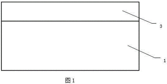
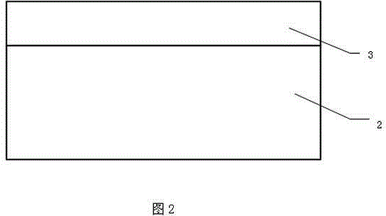
[0042] S1. Thin film coating: the surface of the first plate (1) and the second plate (2) are coated with a layer of low optical refractive index material (3), and the surface coating can be spin coating or coil coating and silk screen coating, the thickness of the coated low optical refractive index material (3) is thicker than the depth of the first groove (5) in step S2 and the depth of the second groove (7) in step S4 . The size of the first pit (5) is the same as that of the second pit (7).

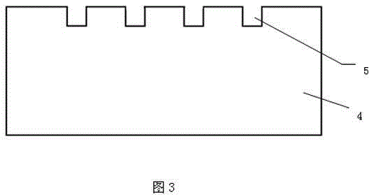
[0043] S2. Manufacture of the main body: the material of the main body (4) is manufactured by traditional photolithography technology or injection molding method. There are first pits (5) of different shap...


PUM


Abstract

The invention discloses a manufacturing method of an optical waveguide embedded optical printed circuit board. The manufacturing method comprises the following steps: coating a thin film, forming grooves by printing and pressing, depositing a metal, coating a second-layer thin film, laminating, punching by laser, and etching, wherein the step of forming grooves by printing and pressing comprises the three substeps of manufacturing a body, forming a mold, and duplicating a shape. No additional optical coupling component is needed for the optical printed circuit board, and the optical waveguide with 45-degree total-reflection mirrors on two ends is embedded into the optical printed circuit board by the grooves formed by printing and pressing, thus the photo-electric conversion efficiency of the optical printed circuit board can be improved, and the procedure of manufacturing the additional optical coupling component is omitted. The manufacturing method disclosed by the invention is suitable for large-scale manufacturing.

Description

technical field [0001] The invention relates to the field of circuit board manufacturing, in particular to an optical waveguide embedded optical printed circuit board with vertical optical coupling capability manufactured by using embossed groove technology. Background technique [0002] In traditional printed circuit boards, signals are mainly transmitted by copper wires. Therefore, loss problems generally occur when the transmission rate exceeds 1Gb / s or above. And as future computer systems increasingly require higher transmission requirements, optical printed circuit boards are a method that can solve the loss problem and provide data rates above 10Gb / s. However, only the optical printed circuit board is not enough. The peripheral supporting equipment such as lasers, optical sensors and optical coupling components need to be integrated with it to take advantage of the optical printed circuit board. Contents of the invention [0003] The object of the present inventio...

Claims


Application Information

Patent Timeline
Patent Type & Authority Applications(China)
IPC IPC(8): G02B6/13
CPCG02B6/13
Inventor 杜子良罗家邦张伟连
Owner 广州依利安达微通科技有限公司
Learn More