Trench-type super-junction device layout structure and manufacturing method thereof

A technology of layout structure and manufacturing method, which is applied in semiconductor/solid-state device manufacturing, semiconductor devices, electrical components, etc., can solve problems such as device failure, and achieve the effect of avoiding wafer warping

Active Publication Date: 2015-05-13
SHANGHAI HUAHONG GRACE SEMICON MFG CORP
View PDF7 Cites 8 Cited by
  • Summary
  • Abstract
  • Description
  • Claims
  • Application Information

AI Technical Summary

Problems solved by technology

[0007] The technical problem to be solved in this application is to solve defects such as dislocations and even device failures caused by warping and stress of wafers with deep grooves in the thermal process, and improve the yield

Method used


Image

  • Trench-type super-junction device layout structure and manufacturing method thereof
  • Trench-type super-junction device layout structure and manufacturing method thereof
  • Trench-type super-junction device layout structure and manufacturing method thereof

Examples


Embodiment Construction

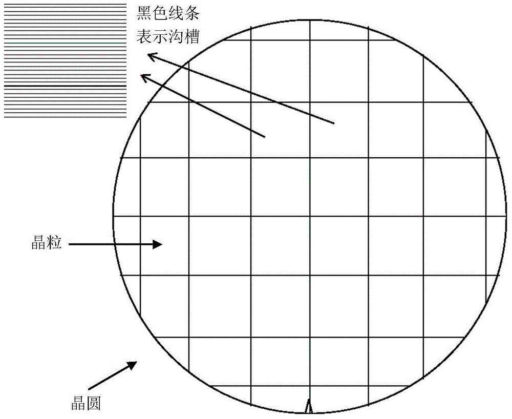
[0018] see Figure 4a , which is Embodiment 1 of the present application. In each die there are multiple trenches for forming pillars, all indicated by black lines. Adjacent and parallel grooves form a plurality of square groove arrays, and the groove arrays are approximately the same size. The arrangement directions of two adjacent groove arrays are perpendicular to each other no matter in the horizontal direction or in the vertical direction.

[0019] see Figure 4b , which is the second embodiment of the present application. It differs from Embodiment 1 only in that the shape of the groove array is either square or rectangular, and the size of the groove array is different.

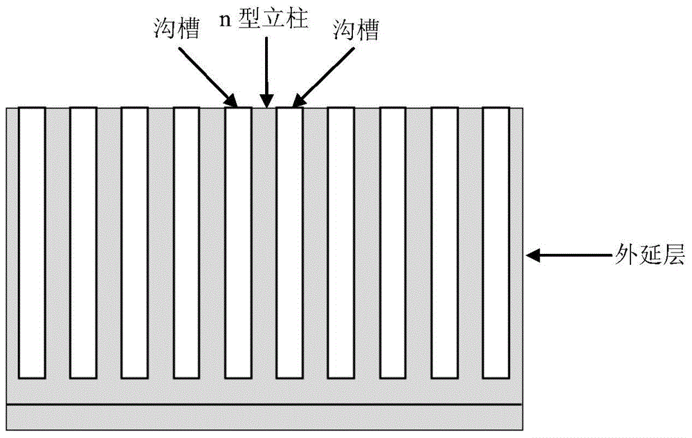
[0020] Since the present application has an array of trenches perpendicular to each other in a crystal grain, the manufacturing process of the layout structure of this special trench-type super junction device is as follows: Figure 5a to Figure 5c As shown, take the manufacture of super junction ...


PUM


Abstract

The invention discloses a trench-type super-junction device layout structure. A plurality of grooves for forming a column in each grain, the adjacent parallel grooves as a groove array, the array direction of the grooves adjacent to each other perpendicular to the array. The present application also discloses a method of manufacturing a trench-type super junction devices, it has formed a super junction structure having two or more of an array of channels in each grain, each groove by adjacent and parallel array composed of grooves, the grooves adjacent to the array direction of the array perpendicular to each other; said method comprising the ion implantation process is formed to cover all the grooves of the array ion-implanted region, ion-implanted region is formed at least one groove parallel to the array and at least another array of channels perpendicular to; final on all array of channels are formed super junction devices. This application is arranged perpendicular to each other by adjacent grains or cell array of channels, and to counteract the stress of deep trenches etched, and overcome the dislocations and other defects.

Description

technical field [0001] The present application relates to a layout structure of a trench type super junction device. Background technique [0002] The Chinese invention patent application with application publication number CN103035677A and application publication date of April 10, 2013 briefly introduces super junction MOSFET (metal-oxide field effect transistor) in the background technology part of its description. In addition to super junction MOSFETs, super junction devices also include super junction JFETs (junction field effect transistors), super junction Schottky diodes, super junction IGBTs (insulated gate bipolar transistors), etc. The common features of these super junction devices are Both have a superjunction structure. [0003] see Figure 1a , which is a structural schematic diagram of an existing super-junction JFET, which has alternately arranged p-type pillars (pillars, also called vertical regions) and n-type pillars in the n-type epitaxial layer. The al...

Claims


Application Information

Patent Timeline
Patent Type & Authority Applications(China)
IPC IPC(8): H01L29/06H01L21/18
CPCH01L21/18H01L29/0692H01L29/0634H01L29/7802
Inventor 李昊
Owner SHANGHAI HUAHONG GRACE SEMICON MFG CORP
Why Eureka
Try Eureka