Power MOSFET device and manufacturing method thereof

A device and power technology, applied in the field of MOSFET devices and their manufacturing, can solve the problem that it is difficult to further improve the withstand voltage of the device terminal area, and achieve the effects of improving processing reliability, avoiding wafer warpage, and improving withstand voltage.

Active Publication Date: 2022-06-07
NANJING MICRO ONE ELECTRONICS +1
View PDF4 Cites 0 Cited by
  • Summary
  • Abstract
  • Description
  • Claims
  • Application Information

AI Technical Summary

Problems solved by technology

Whether it is a single epitaxy or multiple epitaxy process, the device terminal area and the active area are in the same epitaxial layer, it is difficult to further improve the withstand voltage of the device terminal area, making the device face reliability problems

Method used


Image

  • Power MOSFET device and manufacturing method thereof
  • Power MOSFET device and manufacturing method thereof
  • Power MOSFET device and manufacturing method thereof

Examples


Embodiment 1

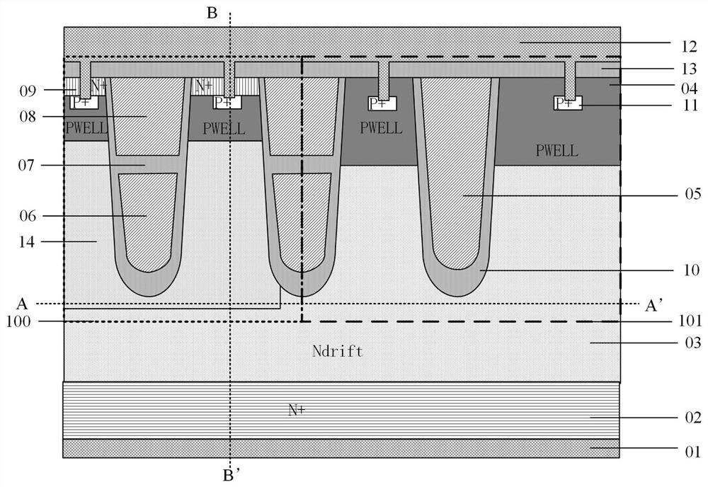
[0037] Refer to appendix Figure 1 , the present invention discloses a power MOSFET device, the power MOSFET device is divided into an active region 100 and a terminal region 101, comprising a drain metal 01, the drain metal 01 is provided with a first conductive type substrate 02, the first conductive type substrate 02 is provided with a first conductive type epitaxial layer 03, the first conductive type epitaxial layer 03 is provided on the first conductive type epitaxial layer 03 is provided with a second conductive type epitaxial layer 04, In the active region 100 of the first conductive type epitaxial layer 03 and the second conductive type epitaxial layer 04 is provided with a first conductive type well region 14.

[0038]In the epitaxial layer of the first conductive type and the epitaxial layer of the second conductive type 04 is provided with a first type groove 07 and a second type groove 10 composed of an insulating material such as silicon dioxide, the first type of gro...

Embodiment 2

[0042] A method for producing a power MOSFET device, including the following steps:

[0043] Step 1: Select the first conductive type substrate 02 material and epitaxially grow the first conductive type epitaxial layer 03 on its surface;

[0044] Step two: Using a mask window, selectively inject the first conductive type ions into the active region 100 on the surface of the first conductive type epitaxial layer 03 to form the first conductive type well region 14;

[0045] Step three: The surface epitaxial layer 03 of the first conductive type is formed by the surface epitaxial layer 04, the first conductive type well region 14 due to the high temperature diffusion of the epitaxial type 04 into the epitaxial layer 04 of the second conductive type;

[0046] Step four: Selectively etch out the first class groove of the active region 100 and the second type of groove 101 of the second type of trench 101 on the upper surface of the epitaxial layer 03 of the second conductive type 03;

...


PUM


Abstract

The invention relates to a power MOSFET (Metal-Oxide-Semiconductor Field Effect Transistor) device and a manufacturing method thereof, the power MOSFET device is divided into an active region and a terminal region, a first conductive type epitaxial layer is arranged on a first conductive type substrate, a second conductive type epitaxial layer is arranged on the first conductive type epitaxial layer, and a second conductive type epitaxial layer is arranged on the second conductive type epitaxial layer. A first conductive type well region is arranged in the first conductive type epitaxial layer and the second conductive type epitaxial layer of the active region, grooves are arranged in the first conductive type epitaxial layer and the second conductive type epitaxial layer, and a first conductive type source electrode and a second conductive type source electrode are arranged in the second conductive type epitaxial layer of the active region. According to the power semiconductor device and the manufacturing method thereof, warping generated in the manufacturing process of the semiconductor wafer can be relieved, the terminal withstand voltage of the power semiconductor device is effectively improved, and the reliability of the power semiconductor device is improved.

Description

Technical field [0001] The present invention relates to a semiconductor device and a method of making it, in particular a MOSFET device and a manufacturing method thereof. Background [0002] Metal Oxide Semiconductor Field-Effect Transistor (MOSFET) is a voltage-controlled electronic device, which generally has three ports: source, gate and drain. For power MOSFETs, because they need to bear a high voltage when they are turned off, a certain chip area is bound to be required to form a depletion layer withstand voltage. In particular, for lateral power MOSFET devices, high-voltage devices are bound to mean a large chip area, resulting in an increase in chip cost, but such devices have the advantage of easy integration. For longitudinal power MOSFET devices, the voltage-resistant part is transferred from lateral to longitudinal, which can greatly reduce the area of the chip. In addition, the field plate technology commonly used in lateral power devices can greatly improve the with...

Claims


Application Information

Patent Timeline
Patent Type & Authority Applications(China)
IPC IPC(8): H01L29/78H01L29/06H01L21/336H01L21/265
CPCH01L29/7811H01L29/7813H01L29/66734H01L29/66484H01L29/7831H01L21/265H01L29/0623
Inventor 朱袁正杨卓黄薛佺朱晨凯
Owner NANJING MICRO ONE ELECTRONICS
Why Eureka
Try Eureka