

Display device, optical assembly, and production method of optical assembly
A technology of optical components and manufacturing methods, applied in the directions of optical components, optics, instruments, etc., can solve the problems of increasing manufacturing costs, complicated processes, etc., and achieve the effect of reducing manufacturing costs
- Summary
- Abstract
- Description
- Claims
- Application Information
AI Technical Summary
Problems solved by technology
Method used
Image

Examples
Embodiment Construction
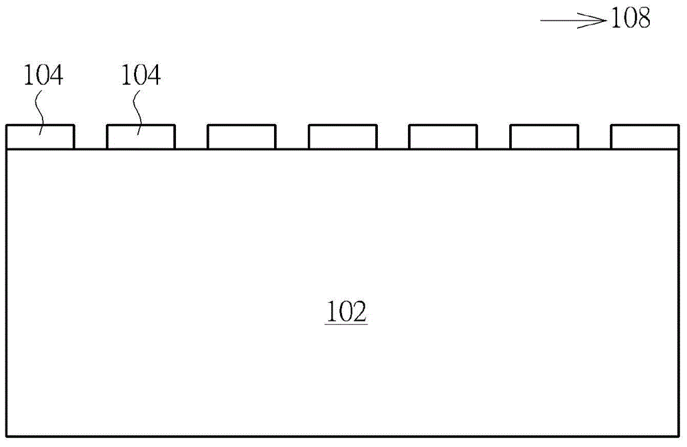
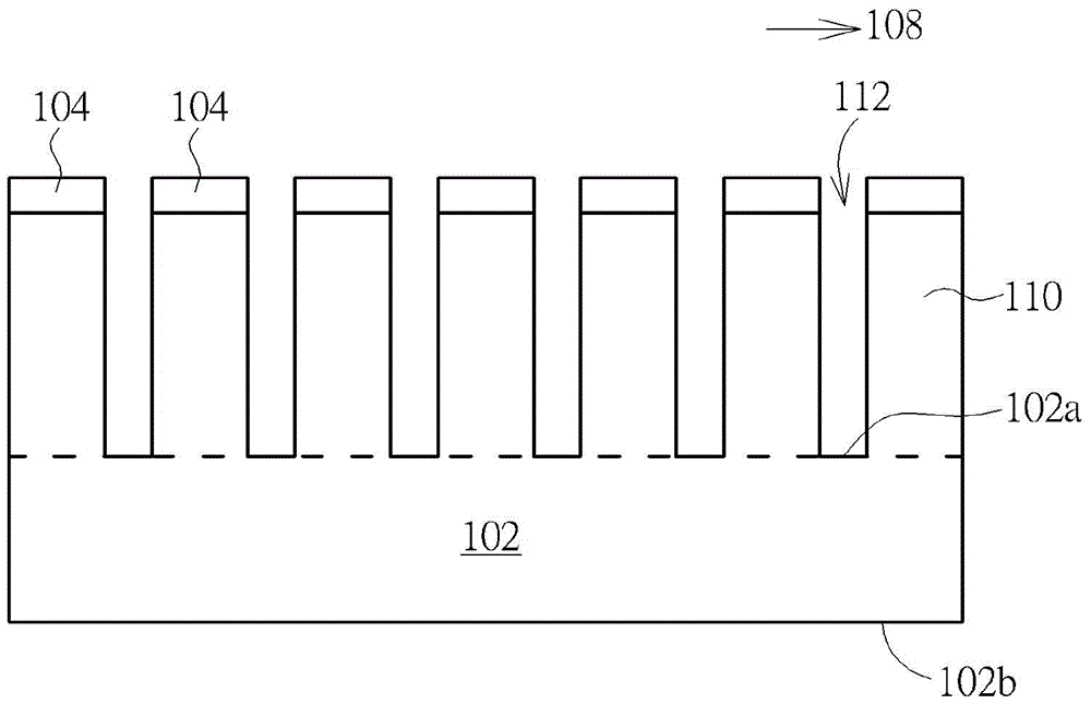
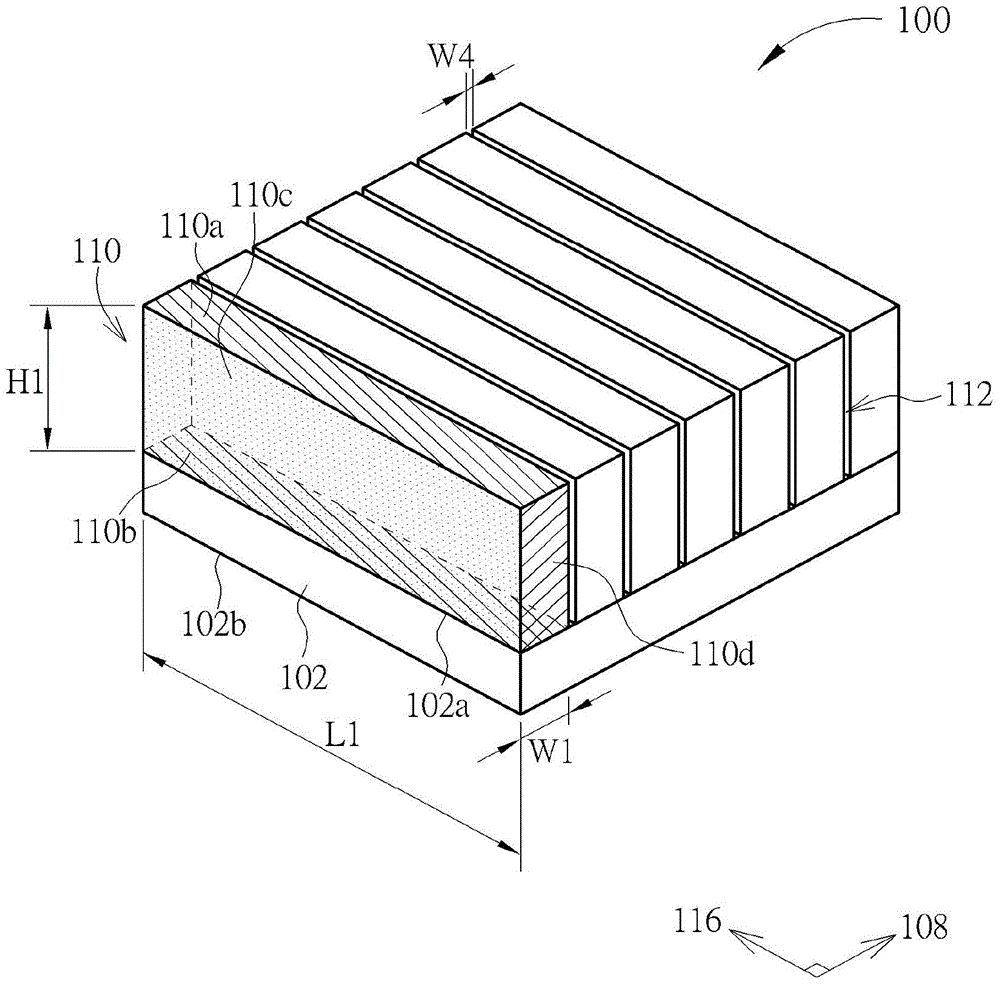
[0036] Please refer to Figure 1 to Figure 3 , Figure 1 to Figure 3 It is a schematic diagram of the manufacturing method of the optical component of the first embodiment of the present invention, wherein image 3 It is a three-dimensional schematic view of the optical assembly of the first embodiment of the present invention. Such as figure 1 As shown, a first transparent substrate 102 such as glass, acrylic or quartz is firstly provided. Then, a first lithography process is performed to form a first photoresist pattern layer 104 on a surface of the first transparent substrate 102, and the first photoresist pattern layer 104 exposes part of the first transparent substrate 102, wherein the first The pattern of a photoresist pattern layer 104 is the same as the top view pattern of the optical component to be formed. In this embodiment, the pattern of the first photoresist pattern layer 104 is a plurality of rectangular blocks arranged along a first direction 108 , but it is...
PUM
| Property | Measurement | Unit |
|---|---|---|
| Width | aaaaa | aaaaa |
Abstract
Description
Claims
Application Information