Image sensor adopting deep groove isolation and manufacturing method thereof

An image sensor and deep trench isolation technology, applied in the field of image sensors, can solve problems affecting the quality of image sensor devices, image sensor device function damage, difficult to remove, etc., to achieve wide selectivity, good surface shape, and eliminate defects effect of influence

Active Publication Date: 2015-05-20
GALAXYCORE SHANGHAI
View PDF7 Cites 17 Cited by
  • Summary
  • Abstract
  • Description
  • Claims
  • Application Information

AI Technical Summary

Problems solved by technology

[0004] The object of the present invention is to provide an image sensor using deep trench isolation and its manufacturing method, so as to solve the problem that the defect of deep trench isolation is difficult to remove. If it is remove

Method used


Image

  • Image sensor adopting deep groove isolation and manufacturing method thereof
  • Image sensor adopting deep groove isolation and manufacturing method thereof
  • Image sensor adopting deep groove isolation and manufacturing method thereof

Examples


Embodiment Construction

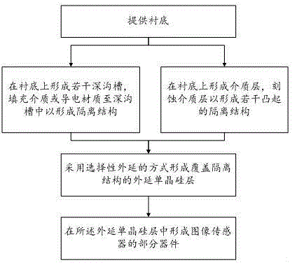
[0027] In the existing image sensor manufacturing process, the deep trench isolation structure is fabricated after the image sensor device is completed. Since the key devices have been formed, various factors such as temperature and environment need to be considered in the subsequent formation of the deep trench isolation structure. , it is necessary to ensure the good interface of the surface of the isolation structure and prevent damage to the device. Because surface defects are brought about during the formation of the isolation structure, the surface defects will lead to the attachment of carriers and increase the noise. Repairing such defects generally requires a variety of special environments such as high temperature, which will affect or even damage the performance of image sensor devices. .

[0028] Therefore, the present invention proposes an image sensor using deep trench isolation and its manufacturing method. Before forming an image sensor device, an isolation str...


PUM


Abstract

The invention provides an image sensor adopting deep groove isolation and a manufacturing method thereof. The method at least comprises the following steps that a substrate is provided; an isolation structure of an isolation pixel unit is formed on the substrate; an epitaxial monocrystalline silicon layer covering the isolation structure is formed in a selective epitaxy mode; partial devices of the image sensor are formed in the epitaxial monocrystalline silicon layer. The deep groove isolation structure is formed before an image sensor device is formed, the isolation structure has better surface shape and fewer defects, in addition, the restoration can be carried out through the epitaxy high-temperature process, and the influence of defects is further eliminated, so that the interface of the isolation structure is more excellent, and the deep groove isolation structure is formed before the device is made, so the selectivity of process means and environment is wider, the damage to the device does not need to be considered, the epitaxial monocrystalline silicon layer is used for forming the device grows after the isolation structure formation, the condition that no stress is conducted into a silicon device is ensured through a high-temperature manufacture procedure, and the performance of the image sensor device is ensured.

Description

technical field [0001] The invention relates to the field of image sensors, in particular to an image sensor using deep trench isolation and a manufacturing method thereof. Background technique [0002] Image sensors can be classified into complementary metal oxide (CMOS) image sensors and charge-coupled device (CCD) image sensors. The advantage of the CCD image sensor is that it has high image sensitivity and low noise, but it is difficult to integrate the CCD image sensor with other devices, and the power consumption of the CCD image sensor is relatively high. In contrast, CMOS image sensors have the advantages of simple process, easy integration with other devices, small size, light weight, low power consumption, and low cost. Therefore, with the development of technology, CMOS image sensors are increasingly used in various electronic products instead of CCD image sensors. At present, CMOS image sensors have been widely used in still digital cameras, camera phones, digi...

Claims


Application Information

Patent Timeline
IPC IPC(8): H01L27/146H01L21/762
Inventor 赵立新杨瑞坤
Owner GALAXYCORE SHANGHAI
Why Eureka
Try Eureka