Optical grating, display device and manufacturing method of optical grating

A manufacturing method and grating technology, applied in chemical instruments and methods, optics, optical components, etc., can solve the problems of light transmittance loss, module thickness, and affecting display effects, etc., and achieve the goal of reducing thickness and light transmission loss Effect

Inactive Publication Date: 2015-05-27
BOE TECH GRP CO LTD +1
View PDF7 Cites 24 Cited by
  • Summary
  • Abstract
  • Description
  • Claims
  • Application Information

AI Technical Summary

Problems solved by technology

This kind of three-dimensional display technology is relatively mature and cheap, and can realize the switching between 2D mode and 3D mode. However, because the existing barrier-bar type 3D display device needs to superimpose a layer of liquid crystal grating on the display panel, the thickness of the liquid crystal grating is usually several About ten millimeters, which leads to a thicker module as a whole; in 2D display, light needs to pass through the liquid crystal layer, so the loss of light transmittance is high, which in turn affects the display effect

Method used


Image

  • Optical grating, display device and manufacturing method of optical grating
  • Optical grating, display device and manufacturing method of optical grating
  • Optical grating, display device and manufacturing method of optical grating

Examples


Embodiment 1

[0110] The manufacturing steps of the 3D liquid crystal display device are as follows:

[0111] Step 1, using a conventional method to manufacture a liquid crystal display panel;

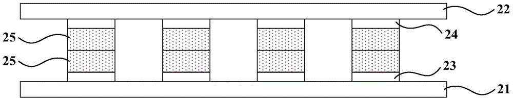
[0112] Step 2. Form a first transparent electrode with a grating structure on the base substrate on the light-emitting side of the liquid crystal display panel. Specifically, an etching process can be used, for example, firstly fabricate an electrode layer covering the substrate surface of the base substrate, and then etch away Part of the electrode layer, forming a first transparent electrode with a grating structure;

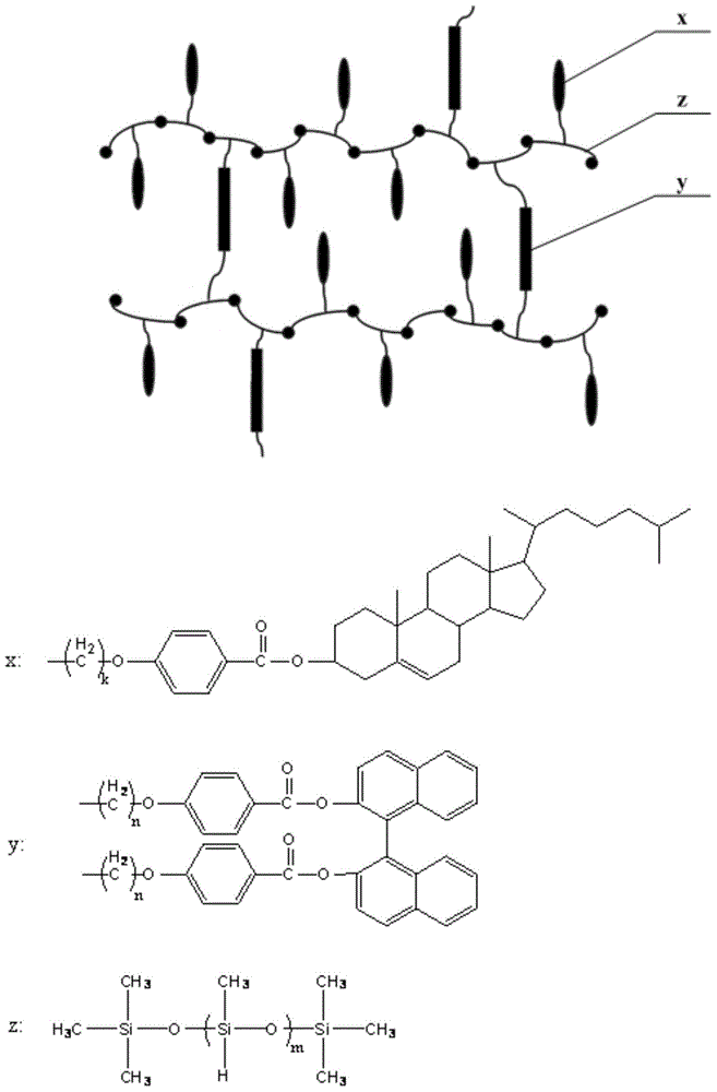
[0113] Step three, will figure 2 As shown n=4 and k=4, the binaphthyldiol crosslinking agent b and the liquid crystalline monomer a are grafted onto the polymethylhydrogensiloxane c of m=6 in a weight ratio of 5:4 to form silicon Oxane side chain liquid crystal elastomer, the obtained siloxane side chain liquid crystal elastomer, ferric oxide nanoparticles, ultraviolet light poly...

Embodiment 2

[0119] The manufacturing steps of the 3D liquid crystal display device are as follows:

[0120] Step 1, using a conventional method to manufacture a liquid crystal display panel;

[0121] Step 2. Form the first layer of transparent electrodes with a grating structure on the light-emitting side substrate of the display panel. Specifically, an etching process can be used. For example, firstly make an electrode layer covering the substrate surface of the substrate, and then etch away part of the electrode layer. an electrode layer, forming a first transparent electrode with a grating structure;

[0122] Step three, will figure 2 As shown n=6 and k=6, the binaphthyldiol crosslinking agent b and the liquid crystalline monomer a are grafted onto the polymethylhydrogensiloxane c of m=4 in a weight ratio of 3:2 to form silicon Oxane side chain liquid crystal elastomer, the obtained siloxane side chain liquid crystal elastomer, ferric oxide nanoparticles, ultraviolet light polymeriz...

Embodiment 3

[0128] The manufacturing steps of the 3D liquid crystal display device are as follows:

[0129] Step 1, using a conventional method to manufacture a liquid crystal display panel;

[0130] Step 2. Form the first layer of transparent electrodes with a grating structure on the light-emitting side substrate of the display panel. Specifically, an etching process can be used. For example, firstly make an electrode layer covering the substrate surface of the substrate, and then etch away part of the electrode layer. an electrode layer, forming a first transparent electrode with a grating structure;

[0131] Step three, will figure 2 As shown n=8 and k=8, the binaphthyldiol crosslinking agent b and the liquid crystalline monomer a are grafted onto the polymethylhydrogensiloxane c with m=10 in a weight ratio of 1:1 to form silicon Oxane side chain liquid crystal elastomer, the obtained siloxane side chain liquid crystal elastomer, ferric oxide nanoparticles, ultraviolet light polyme...


PUM

PropertyMeasurementUnit
thicknessaaaaaaaaaa
thicknessaaaaaaaaaa
thicknessaaaaaaaaaa

Abstract

The invention relates to the technical field of three-dimensional display, and discloses an optical grating, a display device and a manufacturing method of the optical grating. The optical grating comprises a first substrate, a second substrate and a polymer layer, wherein the first substrate and the second substrate are arranged oppositely; a first transparent electrode with an optical grating structure is arranged on one surface, towards the second substrate, of the first substrate; a second transparent electrode, which is arranged corresponding to the first transparent electrode, is arranged on one side, towards the first substrate, of the second substrate; the polymer layer is located between the first transparent electrode and the second transparent electrode, and contains nanoscale materials and a liquid crystal elastomer; the nanoscale materials are capable of transforming electromagnetic energy into heat energy; when voltage is exerted to the first transparent electrode and the second transparent electrode, the electromagnetic energy is transformed into heat energy by the nanoscale materials, the polymer layer is in a cholesteric phase and the reflection wavelength is black; and when voltage is not exerted to the first transparent electrode and the second transparent electrode, the polymer layer is in a transparent state. The optical grating is used for combining with the display panel to realize naked eye 3D (three-dimensional) display; and the transmittance loss in 2D (two-dimensional) display is reduced.

Description

technical field [0001] The invention relates to the technical field of three-dimensional display, in particular to a grating, a display device and a manufacturing method of the grating. Background technique [0002] Among flat panel display devices, Thin Film Transistor Liquid Crystal Display (TFT-LCD for short) has the characteristics of small size, low power consumption, relatively low manufacturing cost and no radiation, and occupies a dominant position in the current flat panel display market. leading position. Liquid crystal displays are more and more widely used in modern life. Common liquid crystal displays can be used as mobile phone display screens, Note Book display screens, GPS display screens, LCD TV display screens, etc. With the advancement of science and technology, because traditional displays can only display flat images, they can no longer meet people's requirements for display quality. Three-dimensional (Three Dimension, 3D for short) display has been ex...

Claims


Application Information

Patent Timeline
Patent Type & Authority Applications(China)
IPC IPC(8): G02F1/29G02F1/1333G02B27/22G02B30/25G02B30/30
CPCG02F1/1333G02F1/29G02B30/30B29D11/0073B29D11/00788G02F1/1347G02F1/31G02F2201/30G02F2201/343G02F2202/36G02F2203/04G02F2203/62H04N13/31G02F1/132G02F1/13718C09K19/408G02B5/3058G02B30/25G02B30/27G02B30/34
Inventor 武晓娟李伟
Owner BOE TECH GRP CO LTD
Why Eureka
Try Eureka