Eureka AIR delivers breakthrough ideas for toughest innovation challenges, trusted by R&D personnel around the world.

High-flatness rigid-flex board provided with ink windows shaped like dual nested rectangles and manufacturing method

A technology of soft and hard combination board and manufacturing method, which is applied in the direction of printed circuit manufacturing, structural connection of printed circuit, printed circuit, etc. It can solve problems such as inconsistent shrinkage force, large deformation of board surface, and influence on flatness, so as to reduce ink area , high flatness, and the effect of reducing warpage

Inactive Publication Date: 2015-05-27
SHENZHEN HUALIN CIRCUIT TECH
View PDF6 Cites 5 Cited by
  • Summary
  • Abstract
  • Description
  • Claims
  • Application Information

AI Technical Summary

Problems solved by technology

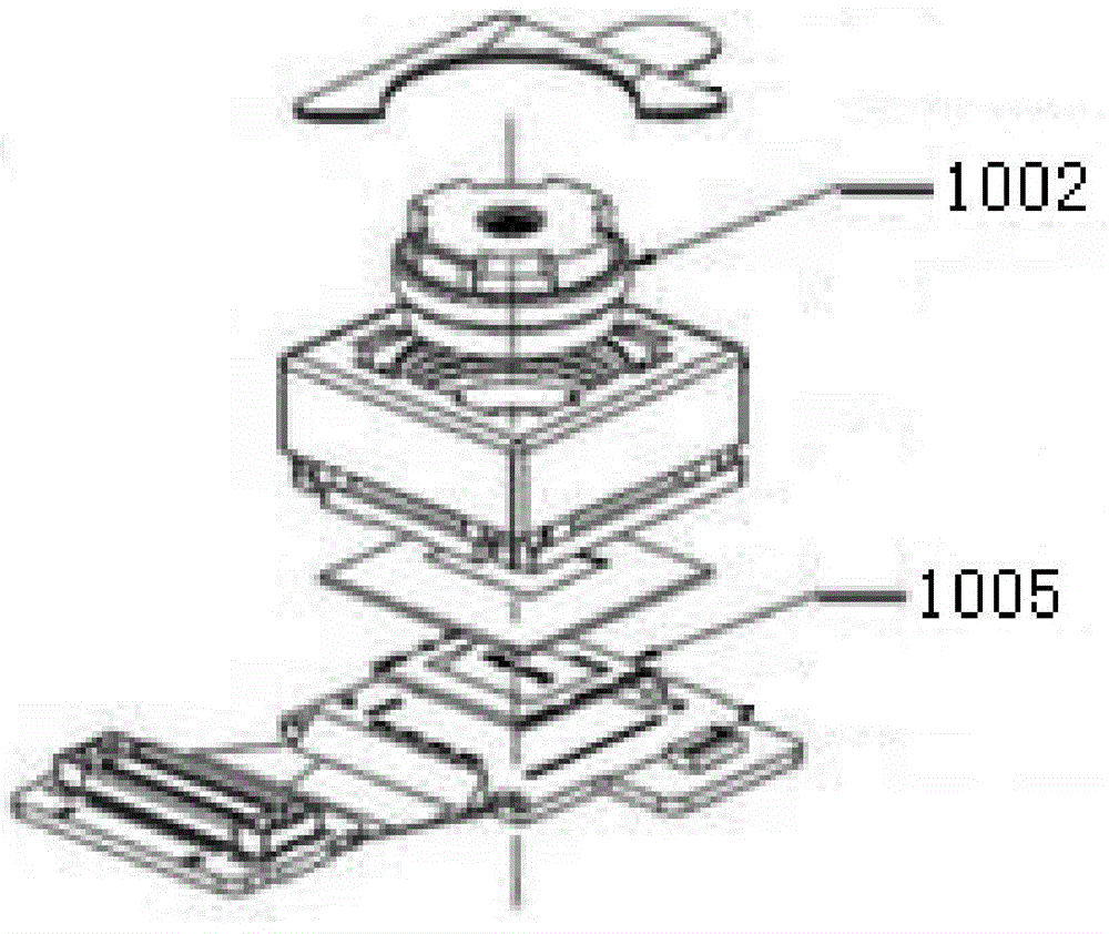
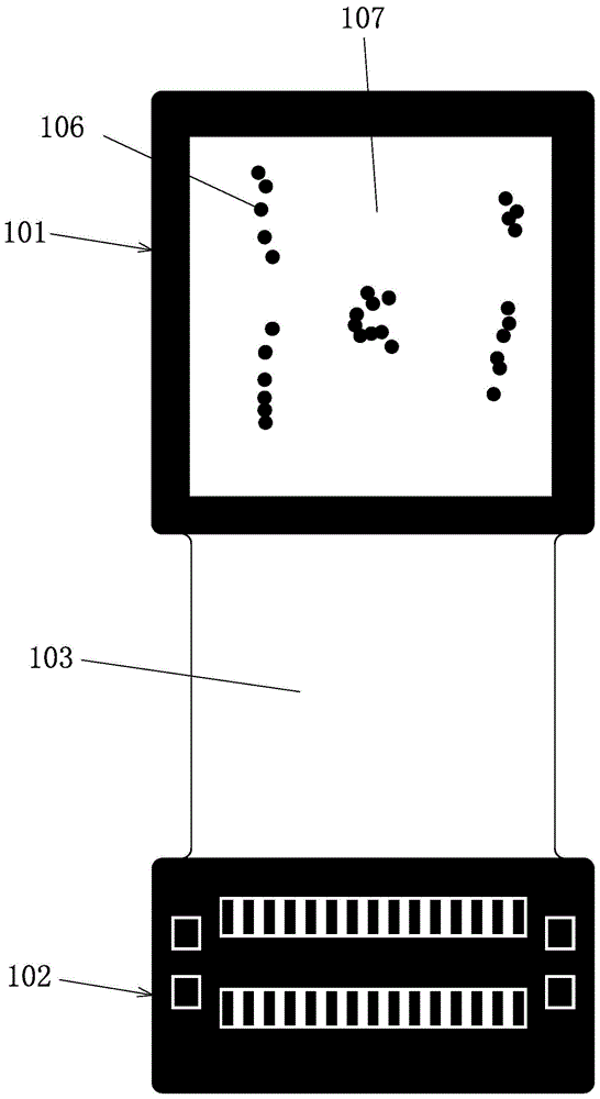
The requirements for flatness are getting higher and higher. At the same time, as the pixels of the camera module are getting higher and higher, the power consumption of the chip is also getting higher and higher, and the heat generated is also increasing. For example, image 3 As shown, most of the hard circuit boards 101 carrying chips are designed with a gold surface 107 on the back of the chip to facilitate chip heat dissipation. Rigid-flex boards with a finished thickness of 0.25-0.45mm have just started in the industry. Due to their thinner thickness, Its overall rigidity is weak, and the board surface is easily deformed during the component mounting process
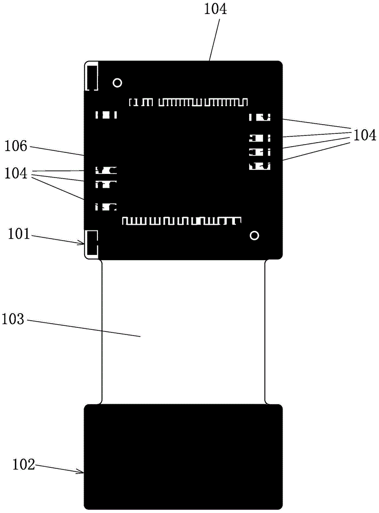
This has a lot to do with the structure of the board, see figure 2 , the main performance is that the solder resist ink 106 on the bonding surface (chip surface) has a relatively large area, accounting for about 80% of the entire chip surface, and there are only a few irregular, small-area common windows 104; The back side of the board is mainly occupied by the gold surface 107 (this side is a gold-plated large copper surface, which is used for grounding and heat dissipation of high-pixel camera products, except for a few via holes that need to be covered with solder resist oil 106 ink, the others are exposed , so the ink coverage area of ​​this surface is about 20%), due to the difference in the area of ​​the solder resist ink on the front and back sides, the shrinkage force of the two sides is inconsistent when the temperature exceeds 260 ° C, and the deformation of the board surface is large, which affects the flatness

Method used


Image

  • High-flatness rigid-flex board provided with ink windows shaped like dual nested rectangles and manufacturing method
  • High-flatness rigid-flex board provided with ink windows shaped like dual nested rectangles and manufacturing method
  • High-flatness rigid-flex board provided with ink windows shaped like dual nested rectangles and manufacturing method

Examples


Embodiment Construction

[0022] Such as Figure 4 and Figure 5 As shown, the flexible and rigid board with high flatness back-type ink window of the present invention includes rigid circuit boards 101, 102 and flexible circuit board 103, and the chip area of ​​the rigid circuit board 101 is silk-screened with solder resist ink 109. The other side of the circuit board 101 opposite to the chip area is also provided with a gold surface 107 for heat dissipation. Only a few via holes on the surface of the gold surface 107 are covered with solder resist ink. Open the window 108 in the shape of back.

[0023] In order to form the back-shaped window 108, the present invention provides a method for manufacturing a high-flatness back-shaped ink window-opening flex-hard board, which includes the following steps: Step 1, rigid circuit boards 101, 102 and flexible circuit board 103 are bonded After the junction is solidified, through drilling, copper plating, circuit making and other processes, the outer circui...


PUM

PropertyMeasurementUnit
Widthaaaaaaaaaa
Thicknessaaaaaaaaaa

Abstract

The invention discloses a high-flatness rigid-flex board provided with ink windows shaped like dual nested rectangles and a manufacturing method. The manufacturing method comprises steps as follows: step 1, solder resist ink covers, is printed on a rigid circuit board of the rigid-flex board in a silk-screen manner and is precured and baked at the low temperature of 80-100 DEG C; step 2, a pattern on a solder mask film is designed to be shaped like dual nested rectangles and is transferred to the solder resist ink for exposure, and the solder resist ink in a black area doesn't have a chemical polymerization reaction and is washed away by a solution of a solder mask developer to form the windows shaped like dual nested rectangles; the solder resist ink located outside a shading area is subjected to illumination exposure, has a chemical polymerization reaction and accordingly is prevented from being washed away by the solution of the solder mask developer, and an ink bridge is formed between every two windows shaped like dual nested rectangles; step 3, high-temperature baking is performed at the temperature of 150-180 DEG C; step 4, surface processing is performed, and electroless gold plating forming is realized. Difference of ink areas on front and reverse surfaces of the rigid-flex board is avoided, and the flatness is high.

Description

technical field [0001] The invention relates to the field of circuit boards for camera modules of digital products such as mobile phones and computers, in particular to a high-flatness soft-hard combination board and a manufacturing method thereof. Background technique [0002] At present, with the continuous advancement of science and technology, people's requirements for quality life are getting higher and higher, digital products are constantly developing towards convenience and light weight, and the installation of high-pixel cameras has become the trend of market development. The convenience and light weight of digital products make the requirements for circuit boards are getting higher and higher, especially the soft and hard combination boards commonly used in camera modules of digital products such as mobile phones and computers. [0003] The carrier boards of consumer-grade high-pixel cameras are mostly rigid-flex boards. The thinner the rigid-flex board, the thinne...

Claims


Application Information

Patent Timeline
IPC IPC(8): H05K3/28H05K1/02H05K1/14
CPCH05K1/0269H05K3/28H05K3/361H05K2201/068H05K2201/10121
Inventor 潘陈华郭瑞明丁爱平陈伟曹涣威
Owner SHENZHEN HUALIN CIRCUIT TECH
Why Eureka
Eureka Blog
Learn More