Standard silicon wafer thickness measuring device

A technology for thickness measurement and silicon wafers, which is applied in the field of standard silicon wafer thickness measurement devices, can solve problems such as low flatness, small thickness, and large area, and achieve high accuracy, easy operation, and good reliability.

Inactive Publication Date: 2015-06-03
CHENGDU BIZ UNITED INFORMATION TECH
View PDF0 Cites 3 Cited by
  • Summary
  • Abstract
  • Description
  • Claims
  • Application Information

AI Technical Summary

Problems solved by technology

Standard silicon wafers have the characteristics of large area, small thickness, fragility, and low flatness. At present, there is no suitable instrument for measuring the thickness of standard silicon wafers, and there is no ready-made equipment available at home and abroad.

Method used


Image

  • Standard silicon wafer thickness measuring device

Examples


Embodiment Construction

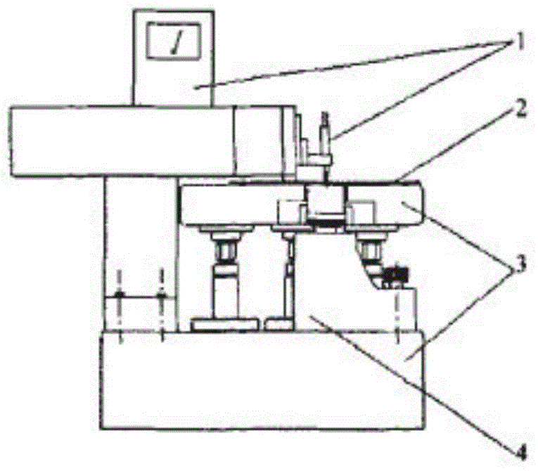
[0009] The standard silicon wafer thickness measuring device consists of three parts: high-precision inductance micrometer, granite frame structure and adjustable ruby ​​spherical table. It is suitable for thickness calibration of standard silicon wafers with a diameter of 305mm (12inch). For standard silicon wafers with different diameters and thicknesses, point-to-point measurement is realized in the direction perpendicular to the surface, and the measurement uncertainty of the calibration standard silicon wafer thickness is 0.2 μm. The granite frame structure is a double-layer workbench. The upper workbench is a silicon wafer bearing platform, which can carry silicon wafers with a diameter greater than 305mm (12inch). The flatness of the work surface is 2μm. The lower workbench is a base with five adjustable support feet It is connected with the upper working platform, and carries the adjustable ruby ​​spherical workbench and the positioning frame of the inductance micromet...


PUM

PropertyMeasurementUnit
Flatnessaaaaaaaaaa

Abstract

The invention relates to a standard silicon wafer thickness measuring device. The standard silicon wafer thickness measuring device consists of a high-precision inductor micrometer, a granite framework structure and a liftable precious stone spherical surface worktable, wherein the granite framework structure is a double-layer worktable, an upper layer working platform is a silicon wafer carrier table for carrying a measured standard silicon wafer, a lower layer worktable is a base, the base is provided with a five adjustable supporting legs which are connected with the silicon wafer carrier table, the liftable precious stone spherical worktable and an inductor micrometer positioning framework are fixedly arranged on the base, the side surface of the inductor micrometer positioning framework is connected with the high-precision inductor micrometer by virtue of threads, the ribbed liftable precious stone spherical worktable with a ruby measuring head and the diameter of 60mm is arranged in the center of the silicon wafer carrier table below the inductor micrometer, the measuring head is right opposite to the center of the lower liftable precious stone spherical surface worktable, and when the thickness of a silicon wafer is measured, the silicon wafer is arranged between the ruby measuring head and the inductor micrometer. The device is suitable for calibration of the thickness of the standard silicon wafer with the diameter less than or equal to 305mm. The standard silicon wafer thickness measuring device has characteristics of compact structure, simplicity in operation, high accuracy and good reliability.

Description

technical field [0001] The invention relates to a measuring device, especially a standard silicon chip thickness measuring device. Background technique [0002] The standard silicon wafer is the standard sample used by each silicon wafer and integrated circuit manufacturer to control the thickness of the silicon wafer during the silicon wafer production process. In the production line, the standard silicon wafer is used as the benchmark, and the thickness of the product silicon wafer is measured by the method of comparative measurement. The manufacturer's standard silicon wafer is put into use after being calibrated by the metrology department. The parameters that need to be measured for standard silicon wafers include: thickness, flatness, and standard graphics of integrated circuits. Standard silicon wafers have the characteristics of large area, small thickness, fragility, and low flatness. At present, there is no suitable instrument for measuring the thickness of stand...

Claims


Application Information

Patent Timeline
IPC IPC(8): G01B7/06
Inventor 曹毅
Owner CHENGDU BIZ UNITED INFORMATION TECH
Why Eureka
Try Eureka