Organic light emitting diode display panel and manufacturing method thereof

A technology of light-emitting diodes and display panels, which is applied in the fields of organic semiconductor devices, semiconductor/solid-state device manufacturing, electrical components, etc., and can solve problems such as glass glue cracks, substrate deformation, and large residual stress

Active Publication Date: 2018-04-06
INNOLUX CORP
View PDF9 Cites 0 Cited by
  • Summary
  • Abstract
  • Description
  • Claims
  • Application Information

AI Technical Summary

Problems solved by technology

If the back plate and cover plate are fixed, great residual stress will be obtained; but if not fixed, it will cause deformation of the substrate
Both the residual stress and the deformation of the substrate will be affected by the destructive vibration of the wheel cutter during the cutting process, resulting in cracking of the glass substrate or cracking or chipping of the glass glue
[0005] Therefore, in order to improve the aforementioned shortcomings, there is an urgent need to develop an organic light-emitting diode panel and its manufacturing method, which can prevent the fatal injury of poor cutting yield due to stress factors without changing the structure of the traditional cutting machine. Improve the cutting yield of the panel and meet the purpose of narrow border at the same time

Method used


Image

  • Organic light emitting diode display panel and manufacturing method thereof
  • Organic light emitting diode display panel and manufacturing method thereof
  • Organic light emitting diode display panel and manufacturing method thereof

Examples


Embodiment Construction

[0028] The implementation of the present invention is illustrated through specific specific examples below, and those skilled in the art can easily understand other advantages and effects of the present invention from the content disclosed in this specification. The present invention can also be implemented or applied through other different specific embodiments, and various modifications and changes can be made to the details in this specification for different viewpoints and applications without departing from the spirit of the present invention.

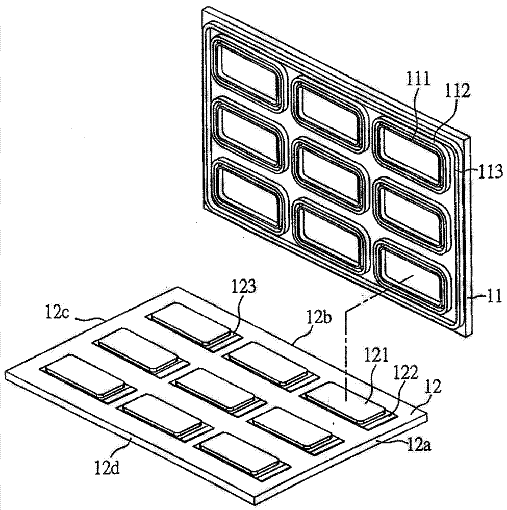
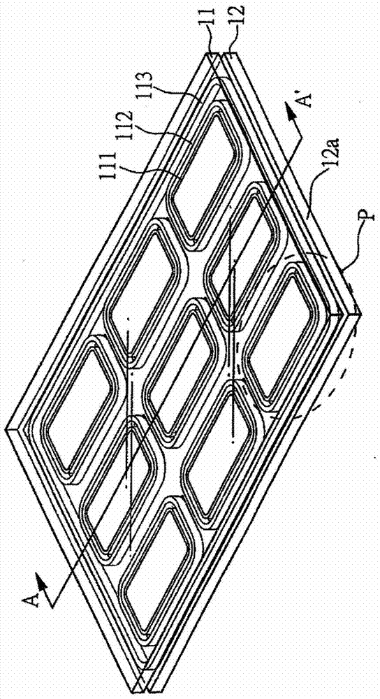
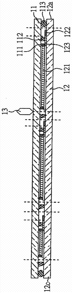
[0029] Please refer to figure 1, which is a schematic view before the first mother substrate and the second mother substrate are assembled in a preferred embodiment of the present invention. Firstly, a first mother substrate 11 and a second mother substrate 12 are provided, both of which are glass substrates. Regarding the first mother substrate 11, firstly, coat at least one glass glue 111 on the first mother substrate 11 with a...


PUM


Abstract

The present invention relates to an organic light emitting diode display panel and a manufacturing method thereof, wherein the organic light emitting diode display panel includes: a first substrate having a first side, a second side, a third side and a A fourth side, wherein the first side is opposite to the third side, and the second side is opposite to the fourth side; a second substrate, disposed opposite to the first substrate; an organic light emitting diode unit , arranged on the second substrate; a glass glue, arranged between the first substrate and the second substrate and arranged around the organic light emitting diode unit; and a buffer unit, arranged between the first substrate and the second substrate and positioned towards the first substrate Between the glass glue on one side and the first side of the first substrate, the buffer unit has a first end, and the first cutting edge of the first end is adjacent to the second side.

Description

technical field [0001] The invention relates to an organic light emitting diode display panel and a manufacturing method thereof, in particular to an organic light emitting diode display panel meeting the requirements of a narrow frame and a manufacturing method thereof. Background technique [0002] Organic light-emitting diodes (OLEDs) have the advantages of light weight, thin thickness, high brightness, fast response, large viewing angle, no need for backlight, low manufacturing cost, and bendability, and have great potential to be applied to various electronic devices Display panels, such as mobile phone panels, car panels, MP3 panels, etc. However, the organic light emitting diode has the disadvantage of not being resistant to moisture, so currently the organic light emitting diode is usually packaged with glass glue to isolate the external moisture. [0003] Generally speaking, OLED devices mostly use glass substrates and are packaged with glass glue (Frit). Although...

Claims


Application Information

Patent Timeline
Patent Type & Authority Patents(China)
IPC IPC(8): H01L27/32H01L51/52H01L51/56
CPCH10K59/127H10K71/851H10K59/8722
Inventor 林敦煌黄浩榕
Owner INNOLUX CORP
Why Eureka
Try Eureka