A low-power organic electroluminescent display device and manufacturing method

A technology of display device and manufacturing method, which is applied in the direction of electric solid state device, semiconductor/solid state device manufacturing, electrical components, etc., can solve the problems of low product yield, complicated process, excessive etching of the second conductive layer, etc. The effect of low, power consumption reduction

Active Publication Date: 2017-02-08
TRULY SEMICON
View PDF4 Cites 0 Cited by
  • Summary
  • Abstract
  • Description
  • Claims
  • Application Information

AI Technical Summary

Problems solved by technology

[0004] However, molybdenum, aluminum and molybdenum are used as the second conductive layer 102 in the first wiring electrode 11 and the second wiring electrode 51. In the process, not only the process is complicated, but also the second conductive layer of the first electrode wiring electrode and the second electrode wiring electrode is often etched too much, resulting in low product yield

Method used


Image

  • A low-power organic electroluminescent display device and manufacturing method
  • A low-power organic electroluminescent display device and manufacturing method
  • A low-power organic electroluminescent display device and manufacturing method

Examples


Embodiment Construction

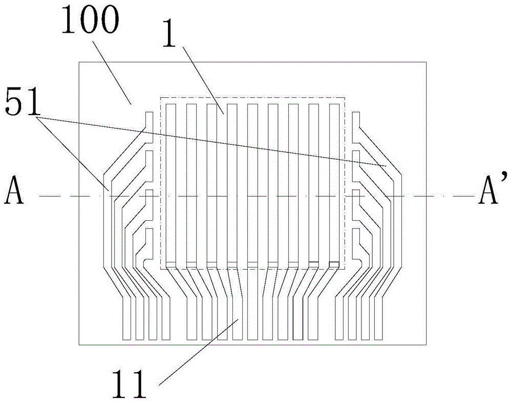
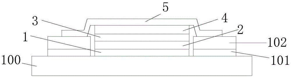
[0034] As described in the background technology, but in the production process of existing OLEDs, especially in the production process of the first electrode wiring electrodes and the second electrode wiring electrodes, not only the process is complicated, but also the first electrode wiring electrodes and the second electrode wiring electrodes often appear. The phenomenon that the second conductive layer of the second electrode wiring electrode is etched too much leads to a low yield rate of the product. The inventor found that the cause of this defect is mainly due to the use of layered exposure etching when making the first electrode wiring electrodes and the second electrode wiring electrodes, that is, the first electrode wiring area and the second electrode wiring area need to be The wiring area is subjected to two exposures and etching, and the position shift is prone to occur in the two exposures and etchings, which leads to the phenomenon that the second conductive lay...


PUM


Abstract

The invention discloses a low-power-consumption organic electroluminescent display device and a manufacturing method. Only one time of exposure is needed for the manufacturing process of a first electrode wiring electrode and a second electrode wiring electrode, then a first transparent conductive layer, a metal layer and a second transparent conductive layer are synchronously etched to form the first electrode wiring electrode and the second electrode wiring electrode, and the phenomenon of lateral erosion caused by deviation due to existing layered exposure etching is avoided. Moreover, the third conductive layer of the organic electroluminescent display device provided by the invention effectively protects the second conductive layer and provides the anti-oxidization capacity of the second conductive layer; since the second conductive layer is a metal layer, the resistance is low, the first conductive layer and the second conductive layer are high-temperature crystallized films and the resistance is low, the power consumption of the organic electroluminescent display device is reduced.

Description

technical field [0001] The invention relates to the technical field of flat panel displays, and more specifically, relates to a low power consumption organic electroluminescent display device and a manufacturing method. Background technique [0002] Organic Electroluminescence Display (OLED) has the characteristic of self-luminescence. It uses a very thin organic material coating and glass substrate. When the current passes, the organic material will emit light. Moreover, the OLED display has a large viewing angle, can be flexible, and can significantly save power, so the OLED display has many advantages that light-emitting diodes cannot match. [0003] combine Figure 1a and 1b as shown, Figure 1a It is a schematic diagram of the electrode layer on the glass substrate of the existing OLED, Figure 1b for Figure 1a The cross-sectional view of the existing OLED along the AA' direction. Among them, the existing OLED includes a glass substrate 100, a first electrode 1 (ano...

Claims


Application Information

Patent Timeline
Patent Type & Authority Patents(China)
IPC IPC(8): H01L51/56H01L27/32
Inventor 谢志生苏君海柯贤军何基强李建华
Owner TRULY SEMICON
Why Eureka
Try Eureka