
Constant trans-conductance bias circuit for C-type inverter

A technology of constant transconductance and bias circuit, which is applied in the direction of instruments, regulating electric variables, control/regulation systems, etc., and can solve inverter quiescent current and bandwidth dependence on power supply voltage, performance loss, inverter bandwidth and slew rate drop and other issues

Active Publication Date: 2015-06-10
SOI MICRO CO LTD
View PDF5 Cites 14 Cited by
  • Summary
  • Abstract
  • Description
  • Claims
  • Application Information

AI Technical Summary

Problems solved by technology

[0004] However, a simple inverter can only provide a very low power supply rejection ratio (PSRR). Due to temperature-induced threshold voltage variation, the unity-gain bandwidth of the inverter will be strongly dependent on temperature. Since it operates in the subthreshold region, when the transistor At the slow process corner, the transconductance and current of the transistor will decrease, and the bandwidth and slew rate of the inverter will be severely reduced, causing performance loss
The quiescent current and bandwidth of the inverter are heavily dependent on the process, power supply voltage, temperature, and the circuit stability decreases

Method used


Image

  • Constant trans-conductance bias circuit for C-type inverter
  • Constant trans-conductance bias circuit for C-type inverter
  • Constant trans-conductance bias circuit for C-type inverter

Examples


Embodiment Construction

[0018] The following will clearly and completely describe the technical solutions in the embodiments of the present invention with reference to the accompanying drawings in the embodiments of the present invention. Obviously, the described embodiments are only some, not all, embodiments of the present invention. Based on the embodiments of the present invention, all other embodiments obtained by persons of ordinary skill in the art without making creative efforts belong to the protection scope of the present invention.

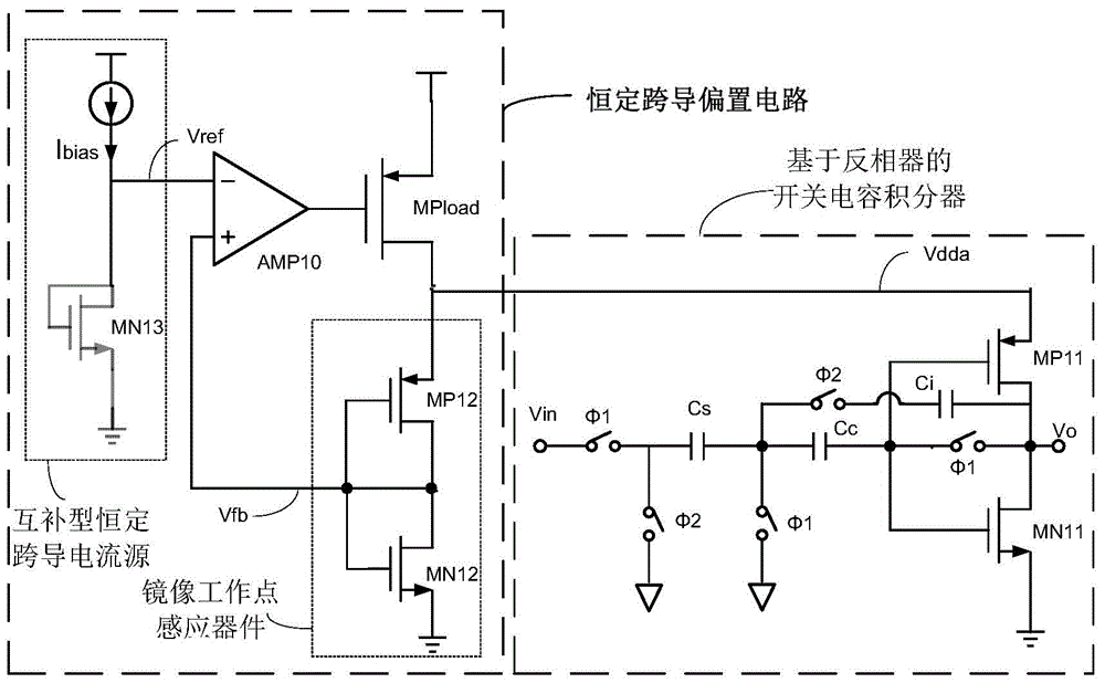
[0019] figure 1 The structure of the constant transconductance bias circuit of the class C inverter according to the embodiment of the present invention is shown. Such as figure 1 As shown, the constant transconductance bias circuit of the C-type inverter includes an inverter-based switched capacitor integrator and a constant transconductance bias circuit; in the inverter-based switched capacitor integrator, the OTA and the The constant transconductance bias...


PUM


Abstract

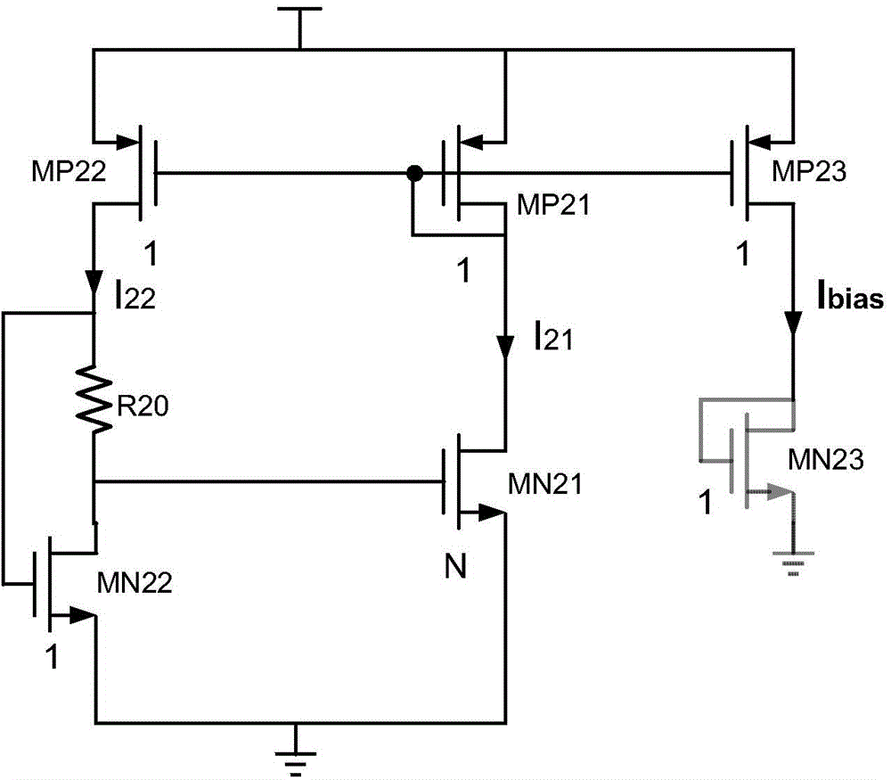
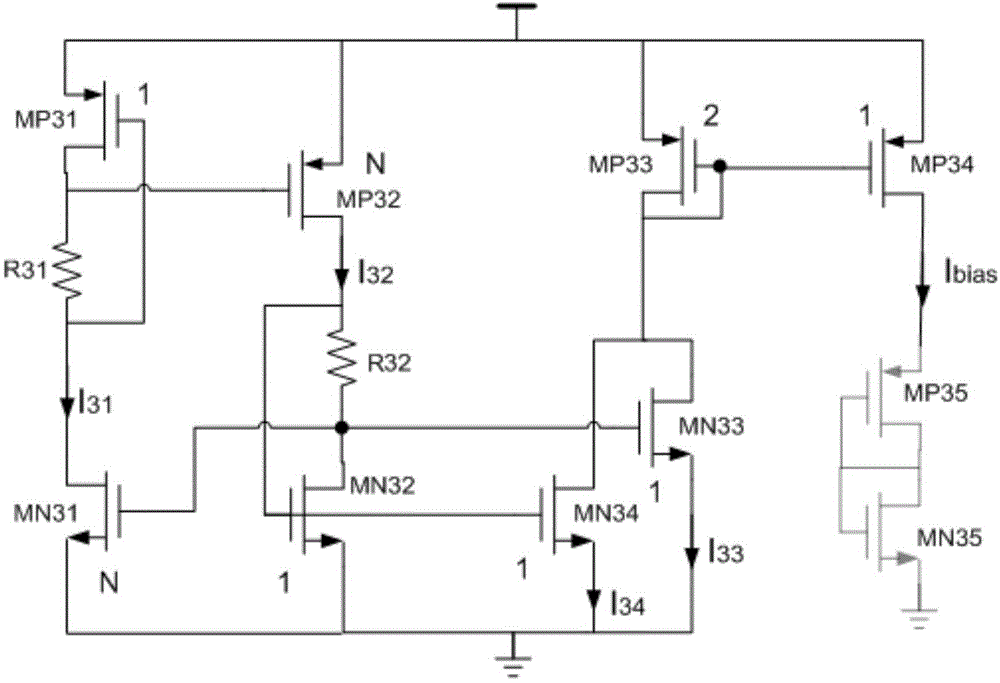
The invention discloses a constant trans-conductance bias circuit for a C-type inverter. The constant trans-conductance bias circuit comprises an inverter-based switched capacitor integrator and a constant trans-conductance bias circuit body, wherein an OTA in the inverter-based switched capacitor integrator is communicated with the constant trans-conductance bias circuit body through a modulating signal Vdda; the inverter-based switched capacitor integrator comprises an inverter composed of a first NMOS transistor and a first PMOS transistor; the constant trans-conductance bias circuit body comprises a mirror working point sensing device, a complementary type constant trans-conductance bias current source, an operational amplifier and an output load transistor; through the complementary constant trans-conductance bias current source, the total trans-conductance of a bias inverter can be constant, and prevented from changing along with the process bias and the temperature of the NMOS transistor and the PMOS transistor. Therefore, the unity-gain bandwidth and built-up time of the inverter can also keep constant when the process bias and the temperature change, and the stability of a circuit can be improved.

Description

technical field [0001] The invention relates to the technical field of integrated circuits, in particular to a constant transconductance bias circuit of a class-C inverter. Background technique [0002] With the development of integrated circuits, the feature size of transistors is getting smaller and smaller, the power supply voltage is reduced, the chip integration level is increased and the operating frequency is increased, and the power consumption per unit chip area is getting higher and higher. With the growth of the mobile and portable device market, the The requirement for low power consumption of integrated circuits is increasing, which puts forward requirements for low-voltage and low-power consumption design. However, as the power supply voltage decreases, the transistor threshold voltage does not decrease proportionally, and the input signal swing decreases, especially for the design of operational transconductance amplifiers (Operational Transconductance Amplifi...

Claims


Application Information

Patent Timeline
Patent Type & Authority Applications(China)
IPC IPC(8): G05F1/56
Inventor 柯强卫宝跃刘昱张海英
Owner SOI MICRO CO LTD
Learn More