Sampling clock generation circuit and analog-digital converter

A technology for generating circuits and sampling clocks, which can be used in analog/digital conversion, analog/digital conversion calibration/testing, code conversion, etc.

Active Publication Date: 2015-06-10
HUAWEI TECH CO LTD
View PDF3 Cites 8 Cited by
  • Summary
  • Abstract
  • Description
  • Claims
  • Application Information

AI Technical Summary

Problems solved by technology

[0006] In order to solve the problem that the existing technology cannot effectively adjust the sampling point timing deviation and reduce the conv

Method used


Image

  • Sampling clock generation circuit and analog-digital converter
  • Sampling clock generation circuit and analog-digital converter
  • Sampling clock generation circuit and analog-digital converter

Examples


Embodiment 1

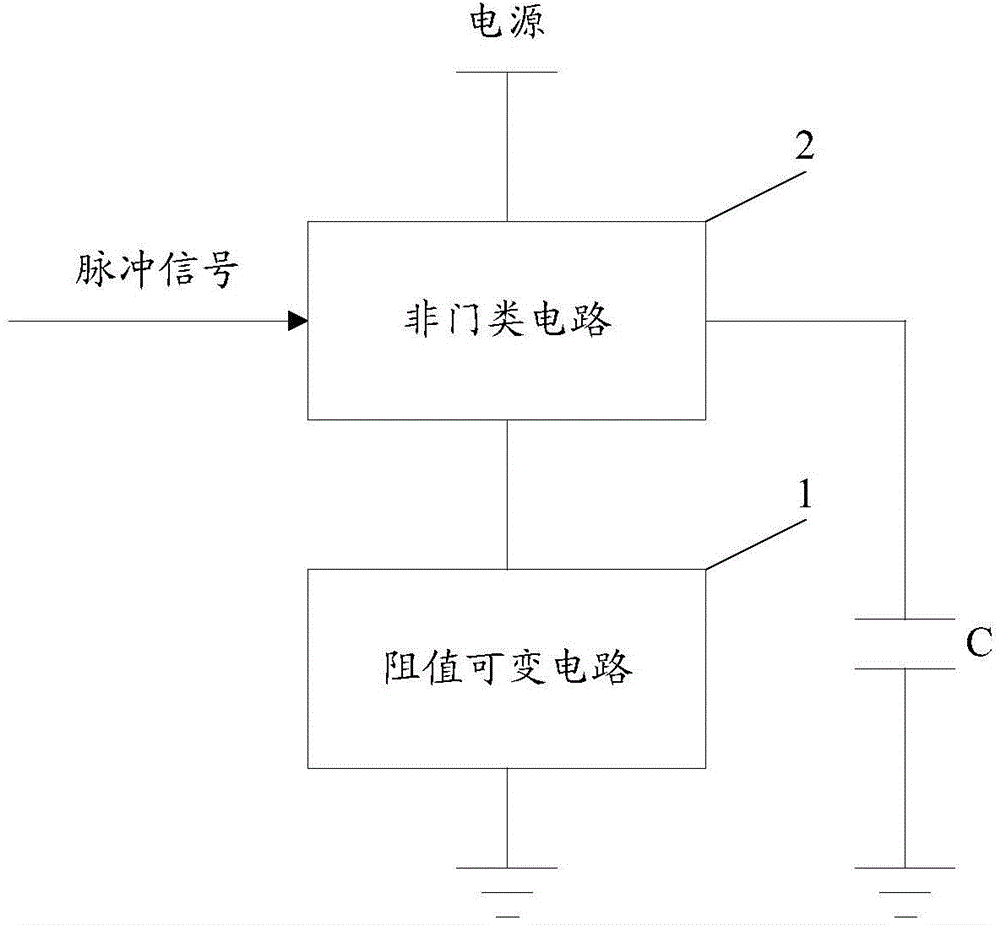
[0051] An embodiment of the present invention provides a sampling clock generation circuit, see image 3 , the sampling clock generating circuit includes a variable resistance circuit 1, a NOT gate circuit 2, and a capacitor C, and the NOT gate circuit 2 includes an input terminal, an output terminal, a power supply terminal and a ground terminal, and the receiving cycle of the input terminal of the NOT gate circuit 2 is The pulse signal of T, the output end of the non-gate circuit 2 is the output end of the sampling clock generation circuit, the output end of the non-gate circuit 2 is connected to one end of the capacitor C, the other end of the capacitor C is grounded, and the power terminal of the non-gate circuit 2 is connected to The power supply, the ground terminal of the NOT circuit 2 is connected to one end of the variable resistance circuit 1, and the other end of the variable resistance circuit 1 is grounded.

[0052] Among them, see Figure 4 , the non-gate circui...

Embodiment 2

[0063] An embodiment of the present invention provides a sampling clock generating circuit. The variable resistance circuit of this embodiment is implemented by using a field effect transistor and a strobe switch. Refer to Figure 7a or Figure 7b , the sampling clock generating circuit includes a variable resistance circuit 1, a NOT gate circuit 2, and a capacitor C, and the NOT gate circuit 2 includes an input terminal, an output terminal, a power supply terminal and a ground terminal, and the receiving cycle of the input terminal of the NOT gate circuit 2 is The pulse signal of T, the output end of the non-gate circuit 2 is the output end of the sampling clock generation circuit, the output end of the non-gate circuit 2 is connected to one end of the capacitor C, the other end of the capacitor C is grounded, and the power terminal of the non-gate circuit 2 is connected to The power supply, the ground terminal of the NOT circuit 2 is connected to one end of the variable resist...

Embodiment 3

[0114] The embodiment of the present invention provides a sampling clock generation circuit, which is different from the second embodiment in that the variable resistance circuit of this embodiment is realized by using one-to-one corresponding resistors and strobe switches, and each resistor corresponds to each The branches after the strobe switches are connected in series are connected in parallel.

[0115] Specifically, such as Figure 12 As shown, the variable resistance circuit 1 may include n resistors R1201-R(1200+n) and n third gating switches K(1201+n) corresponding to the n resistors R1201-R(1200+n) n)-K(1200+2*n), the resistance values ​​of each resistor are different, and each third selection switch includes an input terminal, an output terminal and a control terminal. The branches formed by each resistor in series with the corresponding third select switch are connected in parallel between the ground terminal of the NOT circuit 2 and the ground. The control termi...


PUM


Abstract

The invention discloses a sampling clock generation circuit and an analog-digital converter and belongs to the digital signal processing field. The sampling clock generation circuit comprises a variable-resistance circuit, a NOT gate type circuit and a capacitor, the input end of the NOT gate type circuit receives pulse signals of which the period is T, the output end of the NOT gate type circuit is connected with one end of the capacitor, the other end of the capacitor is connected with the ground, the power supply end of the NOT gate type circuit is connected with a power supply, the ground end of the NOT gate type circuit is connected with one end of the variable-resistance circuit, and the other end of the variable-resistance circuit is connected with the ground; the NOT gate type circuit is used for outputting low level when the pulse signal has high level and outputting high level when the pulse signal has low level; the variable-resistance circuit is used for regularly changing the resistance according to a time length T, the resistance change period is n*T, the resistance is different after each change in each period, and n is an integer larger than or equal to 2. The sampling clock generation circuit and the analog-digital converter enable the conversion accuracy of the ADC to be improved.

Description

technical field [0001] The invention relates to the field of digital signal processing, in particular to a sampling clock generation circuit and an analog-to-digital converter. Background technique [0002] Due to the limitations of technology and device development, the sampling frequency of a single-chip Analog to Digital Converter (ADC) chip cannot be made very high. To achieve a higher sampling frequency, multiple ADC chips can be used in the Interleaved sampling is realized under the driving of sampling clocks with different phases. [0003] Among them, the sampling clocks of different phases are usually realized by the following scheme: the logic circuit divides the clock source signal into n channels, and obtains n channels whose frequency is equal to the frequency of the clock source signal / n and whose phases are different, n≥2 and n is an integer; Different numbers of inverters are connected in series in the transmission channels of n signals for delay, and n sampl...

Claims


Application Information

Patent Timeline
IPC IPC(8): H03M1/10
CPCG06F1/06H03M1/0624H03M1/0836H03M1/1215H03M1/466G06F1/10H03L7/183H03M1/1076
Inventor 杨金达周立人
Owner HUAWEI TECH CO LTD
Why Eureka
Try Eureka