
Oxide thin film transistor (TFT), manufacturing method, array substrate and display device

A technology of oxide thin films and display devices, which is applied in the direction of transistors, semiconductor/solid-state device manufacturing, semiconductor devices, etc., can solve the problems of reduced reliability, instability, and impact on display quality of oxide TFTs, and prevent reflected light from being irradiated To the oxide active layer, improve performance and reliability, improve the effect of display quality

Active Publication Date: 2015-06-17
BOE TECH GRP CO LTD
View PDF6 Cites 5 Cited by
  • Summary
  • Abstract
  • Description
  • Claims
  • Application Information

AI Technical Summary

Problems solved by technology

In order to meet the requirements of large size and high resolution, it is necessary to increase the mobility of the thin film transistor TFT in the display to improve the display effect, but the mobility of the amorphous silicon (a-Si) thin film transistor (Thin Film Transistor, TFT) in the prior art The low efficiency has become a restrictive factor to improve the display effect. Due to its higher mobility than a-Si TFT, oxide TFT has more and more application prospects.
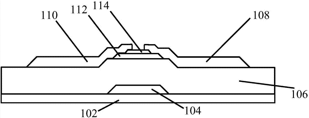
[0003] However, existing oxide TFTs such as figure 1 As shown, it includes: a substrate 102, a gate 104, a gate insulating layer 106, a drain layer 108, a source layer 110, an oxide active layer 112, and an etch stop layer 114 formed sequentially on the substrate 102, from figure 1 It can be seen from the figure that the oxide active layer 112 is between the drain layer 108 and the source layer 110. During the manufacture and use of the oxide TFT, the side leakage or exposure reflection of other processes (such as exposure and development) Light or external light can be reflected at the source layer 110, drain layer 108 interface, that is, reflected between the source layer 110 and the grid 104, the drain layer 108 and the grid 104, when the reflected light irradiates When it comes to the oxide active layer 112, since the Indium Gallium Zinc Oxide (IGZO) used in the oxide active layer 112 is not stable, it is easy to cause leakage current of the oxide active layer when it is irradiated by external light. Increase, which reduces the reliability of oxide TFT and affects the display quality
[0004] In summary, in the prior art, non-perpendicularly incident light such as side leakage light, exposure reflected light, or external light can be reflected between the source layer and the gate, and between the drain layer and the gate. When the reflected light hits the oxide, there is When the source layer is used, it is easy to cause the leakage current of the oxide active layer to increase, which reduces the reliability of the oxide TFT and affects the display quality.

Method used


Image

  • Oxide thin film transistor (TFT), manufacturing method, array substrate and display device
  • Oxide thin film transistor (TFT), manufacturing method, array substrate and display device

Examples


Embodiment Construction

[0026] The specific implementation manners of an oxide thin film transistor TFT, a manufacturing method, an array substrate, and a display device provided by the embodiments of the present invention will be described in detail below with reference to the accompanying drawings.

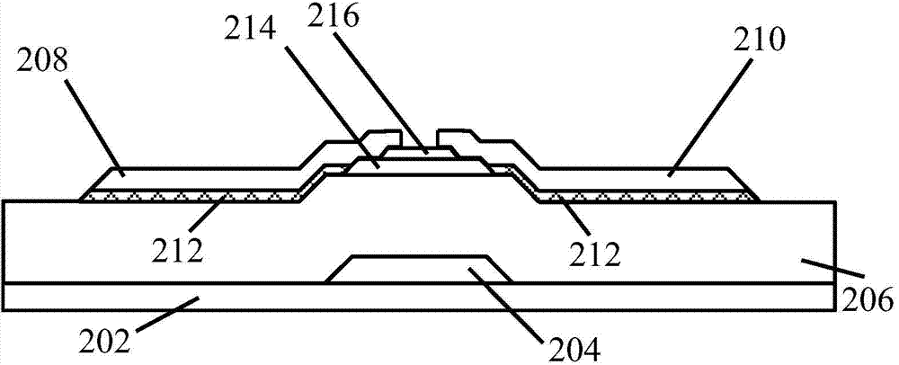
[0027] An oxide thin film transistor TFT provided by an embodiment of the present invention, such as figure 2 As shown, it includes: a substrate 202, a gate 204 sequentially formed on the substrate 202, a gate insulating layer 206, a source layer 208, a drain layer 210, between the gate insulating layer 206 and the source layer 208, and Between the gate insulating layer 206 and the drain layer 210 , a light shielding layer 212 is further included.

[0028] In the oxide TFT provided in the embodiment of the present invention, by forming a light-shielding layer between the gate insulating layer and the source layer and between the gate insulating layer and the drain layer of the oxide thin film transist...


PUM


Abstract

The invention discloses an oxide thin film transistor (TFT), a manufacturing method, an array substrate and a display device. The oxide TFT, the manufacturing method, the array substrate and the display device are used for preventing lateral leakage light or exposure reflected light or external light from being reflected on a source layer interface and a drain layer interface, thereby reducing the influences of the light on an oxide active layer and improving the performance and dependability of the oxide TFT. The oxide TFT comprises a substrate, a gate, a gate insulation layer, a source layer and a drain layer, wherein the gate, the gate insulation layer, the source layer and the drain layer are formed on the substrate in sequence. The oxide TFT is characterized by further comprising shading layers between the gate insulation layer and the source layer and between the gate insulation layer and the drain layer.

Description

technical field [0001] The invention relates to the field of display technology, in particular to an oxide thin film transistor TFT, a manufacturing method, an array substrate, and a display device. Background technique [0002] At present, flat-panel displays have occupied a dominant position in the display market, and are developing towards large-size and high-resolution. In order to meet the requirements of large size and high resolution, it is necessary to increase the mobility of the thin film transistor TFT in the display to improve the display effect, but the mobility of the amorphous silicon (a-Si) thin film transistor (Thin Film Transistor, TFT) in the prior art The low efficiency has become a restrictive factor to improve the display effect. Due to its higher mobility than a-Si TFT, the oxide TFT has more and more application prospects. [0003] However, existing oxide TFTs such as figure 1 As shown, it includes: a substrate 102, a gate 104, a gate insulating lay...

Claims


Application Information

Patent Timeline
IPC IPC(8): H01L29/786H01L29/423H01L29/417H01L21/336
Inventor 何璇吴俊纬刘兴东
Owner BOE TECH GRP CO LTD
Learn More