Supercharge Your Innovation With Domain-Expert AI Agents!

Packaging structure for aligning optical fiber and chip and optical fiber alignment method

A packaging structure and optical fiber alignment technology, applied in the field of communication, can solve the problems of high cost, time-consuming, and increased processing man-hours, and achieve the effects of low cost, reduced manufacturing cost, and large volume

Active Publication Date: 2016-10-05
HUAWEI TECH CO LTD
View PDF6 Cites 0 Cited by
  • Summary
  • Abstract
  • Description
  • Claims
  • Application Information

AI Technical Summary

Problems solved by technology

This method is very time consuming, and as the number of fibers increases, the required processing man-hours also increase almost linearly
High cost

Method used


Image

  • Packaging structure for aligning optical fiber and chip and optical fiber alignment method
  • Packaging structure for aligning optical fiber and chip and optical fiber alignment method
  • Packaging structure for aligning optical fiber and chip and optical fiber alignment method

Examples


Embodiment Construction

[0037] The following will clearly and completely describe the technical solutions in the embodiments of the present invention with reference to the drawings in the embodiments of the present invention.

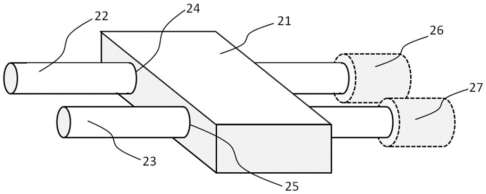
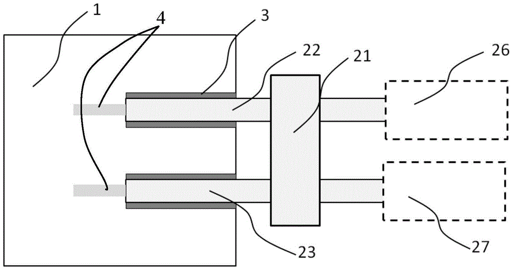
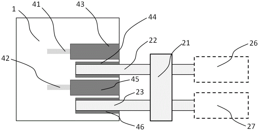
[0038] see figure 1 and figure 2 , the present invention provides a packaging structure in which an optical fiber is aligned with a chip, including a chip 1, a fixing member 21 and at least two optical fibers 22, 23, figure 1 and figure 2 In the illustrated embodiment, two optical fibers 22 and 23 are taken as an example for illustration. In essence, the packaging structure in which the optical fiber and the chip are aligned in the protection of the present invention may include multiple optical fibers. The chip 1 is provided with at least two optical waveguide interfaces 4 for input and output of optical signals. Likewise, figure 1 and figure 2 In the illustrated embodiment, two optical waveguide interfaces 4 are taken as an example for illustration. In essence, the nu...


PUM


Abstract

The invention discloses an optical fiber and chip aimed packaging structure. The packaging structure comprises a chip, a fixed piece and at least two optical fibers, wherein the chip is provided with at least two optical waveguide interfaces used for inputting and outputting optical signals, at least two through holes are formed in the fixed part, and certain end of each of at least two optical fibers is connected with one of other optical devices; the at least two optical fibers respectively penetrate through at least two through holes, the two optical fibers are fixed to form an optical fiber component through the fixed part, and the other ends of the at least two optical fibers are respectively contacted and fixed with the end planes of the optical waveguide interfaces, so as to form optical waveguide coupling between the optical fibers and the optical waveguide interfaces. The invention further provides an optical fiber aiming method. The optical fiber and chip aimed packaging structure and the optical fiber aiming method provided by the invention are simple to operate and low in manufacturing cost.

Description

technical field [0001] The invention relates to the field of communication technology, in particular to a packaging structure for aligning an optical fiber and a chip and an optical fiber alignment method. Background technique [0002] Silicon photonics technology refers to the technology of integrating various functional devices based on planar optical waveguides on silicon materials. This technology mainly uses silicon-on-insulator (SOI) wafers as the substrate. Silicon materials may replace the III / V group materials used in the field of traditional optical devices (the so-called III-V group compounds are B, Al, Ga, In and N, P, As, Compounds formed by Sb, mainly including gallium arsenide (GaAs), indium phosphide (InP) and gallium nitride, etc.), realize miniature, low-power, low-cost optical devices, and are used in computer interconnection, communication networks, and transmission senses etc. Based on silicon photonics technology, optical devices can be directly inte...

Claims


Application Information

Patent Timeline
Patent Type & Authority Patents(China)
IPC IPC(8): G02B6/36
CPCG02B6/3616G02B6/3636
Inventor 陈侠朱以胜清水淳一
Owner HUAWEI TECH CO LTD
Features
  • R&D
  • Intellectual Property
  • Life Sciences
  • Materials
  • Tech Scout
  • Unparalleled Data Quality
  • Higher Quality Content
  • 60% Fewer Hallucinations
Learn More