Preparation method of organic light-emitting diode array

A technology of light-emitting diodes and arrays, applied in the direction of organic semiconductor devices, semiconductor/solid-state device manufacturing, electrical components, etc., can solve the problems of complex preparation process and high cost, achieve simple preparation process, low cost, avoid mask and high temperature vacuum conditional effect

Active Publication Date: 2015-07-01
TSINGHUA UNIV +1
View PDF3 Cites 5 Cited by
  • Summary
  • Abstract
  • Description
  • Claims
  • Application Information

AI Technical Summary

Problems solved by technology

[0004] However, the method of forming the organic light-emitting layer in the prior art is usually vapor deposition, which not only requires a mask, but also requires high-temperature vacuum conditions
Therefore, the preparation process is complicated and the cost is high

Method used


Image

  • Preparation method of organic light-emitting diode array
  • Preparation method of organic light-emitting diode array
  • Preparation method of organic light-emitting diode array

Examples


Embodiment Construction

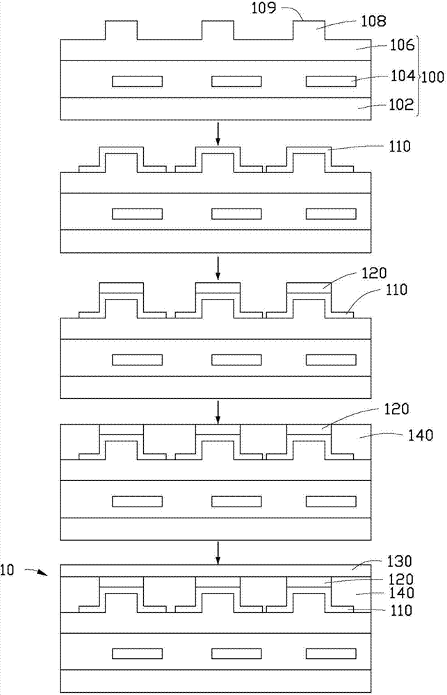
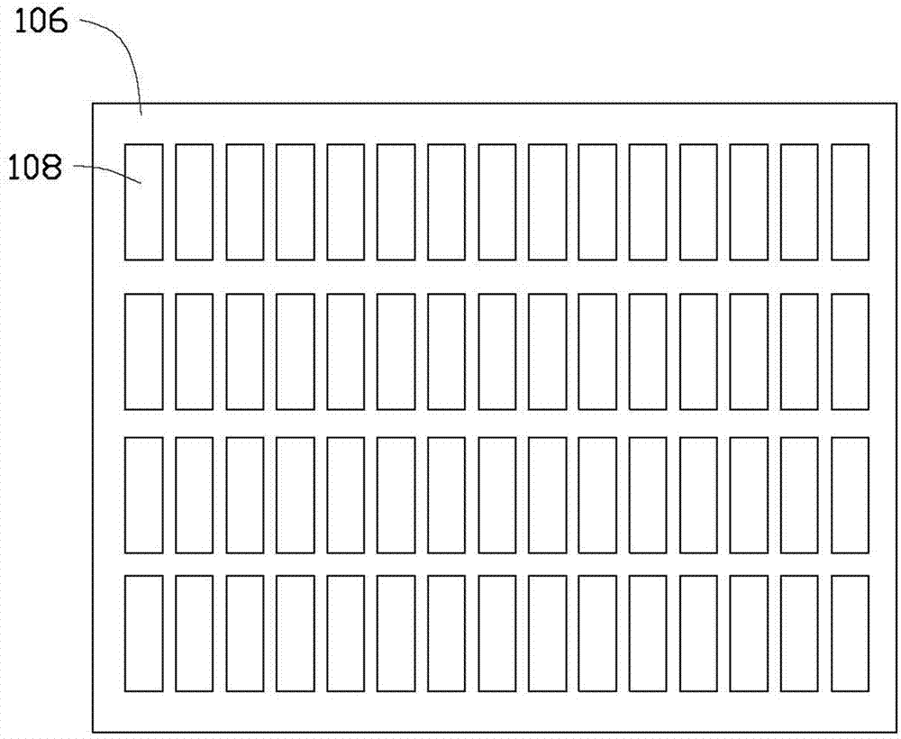
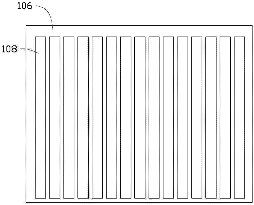
[0039] The present invention provides an organic light emitting diode array, which includes a substrate with a plurality of protrusions and a plurality of organic light emitting diodes arranged on the substrate, wherein each organic light emitting diode includes a stacked first electrode, an organic light emitting layer and a second electrode. The organic light-emitting layer includes a stacked hole injection layer (HIL, Hole Injection Layer), a hole transport layer (HTL, Hole Transport Layer), an electroluminescent layer (EL, Electroluminescent Layer), and an electron transport layer (ETL, Electron Transport Layer) and electron injection layer (EIL, Electron Injection Layer), in which, except for the electroluminescence layer, other layers are optional structures. The plurality of organic light emitting diodes may share a hole injection layer, a hole transport layer, an electron transport layer, and an electron injection layer. The organic light emitting diode array may be a...


PUM


Abstract

The disclosure relates to a method of making organic light emitting diode array. A base defining a plurality of convexities is provided. A number of first electrodes are applied on the plurality of convexities. A patterned second insulative layer is made among the convexities to cover first parts of the first electrodes between the convexities and expose second parts of the first electrodes on top surfaces of the convexities to form a number of protrudent portions. A number of electroluminescent layers are transfer printed on the number of protrudent portions to form a number of organic light emitting layers. A second electrode is electrically connected to the number of organic light emitting layers.

Description

technical field [0001] The invention relates to an organic light emitting diode (OLED) array and a preparation method thereof. Background technique [0002] Organic light-emitting diodes have the characteristic of self-illumination. Therefore, a display screen using organic light-emitting diodes does not need a backlight source, which can significantly save power. Moreover, the display screen using organic light emitting diodes has a large viewing angle, so organic light emitting diodes have become a research hotspot. [0003] In the prior art, a plurality of OLEDs are usually prepared on a substrate to form an array. Wherein, the preparation method of the organic light emitting diode array includes: preparing a thin film transistor (TFT) array on a substrate; forming a first insulating layer on the thin film transistor array; forming a plurality of first insulating layers on the first insulating layer. Electrodes; forming a second insulating layer on the first insulating ...

Claims


Application Information

Patent Timeline
Patent Type & Authority Applications(China)
IPC IPC(8): H01L27/32H01L51/52H01L51/56
CPCH01L51/0013H01L27/3216H01L51/5088H01L51/0017H01L51/5072H01L51/5068H01L51/0023H01L51/5036H01L27/3262H10K59/35H10K59/124H10K59/17H10K59/122H10K71/18H10K50/80H10K50/813H10K50/822H10K59/1201H10K2102/351
Inventor 简良能郑荣安安东朱振东林昌廷吴逸蔚李群庆范守善
Owner TSINGHUA UNIV
Why Eureka
Try Eureka