

Semiconductor device and manufacturing method thereof
A semiconductor and device technology, applied in the field of FinFET semiconductor devices
- Summary
- Abstract
- Description
- Claims
- Application Information
AI Technical Summary
Problems solved by technology
Method used
Image

Examples
Embodiment Construction
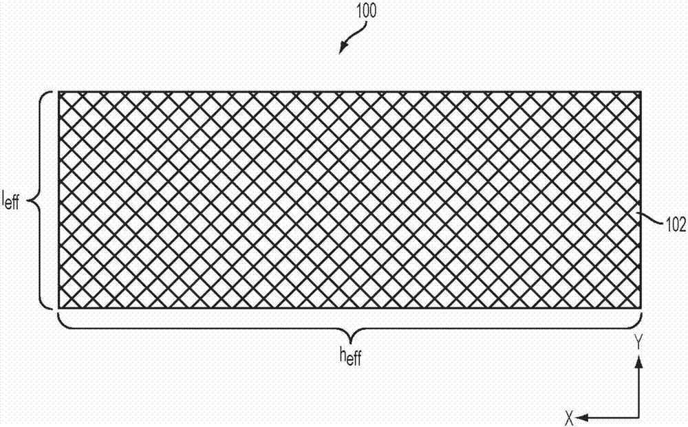
[0029] refer to figure 2 The semiconductor structure 100 includes a bulk semiconductor substrate 102 extending along an X-axis to define a height, and extending along a Y-axis perpendicular to the X-axis to define a length. The bulk semiconductor substrate 102 may be formed of a semiconductor material such as silicon (Si).
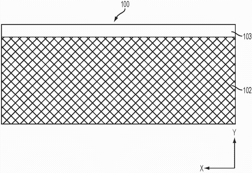
[0030] turn to image 3 , a hard mask layer 103 is formed on the upper surface of the bulk semiconductor substrate 102 . The hard mask layer 103 may be formed using chemical vapor deposition (CVD), and may be formed of a nitride mask material, as would be understood by those of ordinary skill in the art.
[0031] refer to Figure 4 , forming the core layer 104 on the upper surface of the hard mask layer 103 . The core layer 104 can be made of silicon oxide (SiO 2 ) CVD formation. Further, the core layer 104 may be formed of a material different in composition from the hard mask layer 103 to achieve etch selectivity. Materials for the core layer 104 ...
PUM
 Abstract
Description
Claims
Application Information