High-voltage MOSFET current sampling circuit

A current sampling and MOS tube technology, applied in the direction of measuring current/voltage, measuring electrical variables, measuring devices, etc., can solve the problems of poor adaptability to different input voltages, power loss, etc., and achieve the effect of improving accuracy and reducing production costs

Active Publication Date: 2015-07-08
深圳市英特源电子有限公司
View PDF5 Cites 6 Cited by
  • Summary
  • Abstract
  • Description
  • Claims
  • Application Information

AI Technical Summary

Problems solved by technology

[0004] The purpose of the present invention is to provide a high-voltage MOSFET current sampling circuit to meet the power management requirements of high-voltage input...

Method used


Image

  • High-voltage MOSFET current sampling circuit
  • High-voltage MOSFET current sampling circuit
  • High-voltage MOSFET current sampling circuit

Examples


Embodiment 1

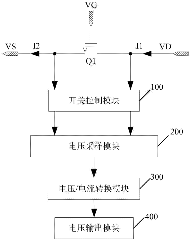
[0023] image 3 It is a block diagram of a current sampling circuit in an embodiment of the present invention. In this embodiment, the current sampling circuit is directly electrically connected to the first terminal and the second terminal of the MOSFET switching device Q1, and the voltage difference between the first terminal and the second terminal of the MOSFET switching device Q1 is used to determine the voltage of the MOSFET switching device Q1. current value. Specifically, the current sampling circuit includes a switch control module 100, a voltage sampling module 200, a voltage / current conversion module 300, and a voltage output module 400, wherein:

[0024] The switch control module 100 is electrically connected to the first terminal and the second terminal of the MOSFET switching device Q1, and is turned on or off according to the first timing signal EN, and is used to control the sampling time point of the current sampling circuit, so as to satisfy the requirements...

Embodiment 2

[0030] Such as Figure 4 , 5 As shown, a current sampling circuit of a high-voltage power N-channel MOSFET switching device Q1 includes a switch control module 100a, a voltage sampling module 200a, a voltage / current conversion module 300a, and a voltage output module 400a, wherein:

[0031] The switch control module 100a includes a first high-voltage power PMOS transistor HVMP1, a second high-voltage power PMOS transistor HVMP2, and a third high-voltage power PMOS transistor HVMP3: the source of the first high-voltage power PMOS transistor HVMP1 and the source of the second high-voltage power PMOS transistor HVMP2 Both are electrically connected to the source of the N-channel MOSFET switching device Q1, the source of the third high-voltage power PMOS transistor HVMP3 is connected to the drain of the N-channel MOSFET switching device Q1, and the first, second and third high-voltage power PMOS The gates of the tubes (HVMP1, HVMP2, HVMP3) are all controlled by the first timing s...

Embodiment 3

[0063] Such as Image 6 As shown, a current sampling circuit of a high-voltage power N-channel MOSFET switching device Q1 includes a switch control module 100b, a voltage sampling module 200b, a voltage / current conversion module 300b, and a voltage output module 400b. from Image 6 It is easy to see that the difference between the third embodiment and the second embodiment is that the components of the switch control module 100b are replaced by replacing the P-channel MOS transistors used in the second embodiment with N-channel MOS transistors. details as follows:

[0064] The switch control module 100b includes a first high-voltage power NMOS transistor HVMN1, a second high-voltage power NMOS transistor HVMN2, and a third high-voltage power NMOS transistor HVMN3: the drain of the first high-voltage power NMOS transistor HVMN1 and the drain of the second high-voltage power NMOS transistor HVMN2 Both are electrically connected to the source of the N-channel MOSFET switching d...


PUM


Abstract

The invention discloses a high-voltage MOSFET current sampling circuit which comprises an on-off control module, a voltage sampling module, a voltage/current conversion module and a voltage output module. The on-off control module controls a sampling time point of the current sampling circuit. The voltage sampling module obtains sampling voltage. The voltage/current conversion module converts the sampling voltage into sampling currents, and then the voltage output module outputs the corresponding voltage. According to the high-voltage MOSFET current sampling circuit, the voltage difference between a drain electrode and a source electrode of a high-voltage power MOSFET switching device is directly sampled so as to judge the currents flowing through the high-voltage power MOSFET switching device, and the problem that due to the fact that in the traditional technology, a sampling element is additionally arranged, power loss is caused is solved; meanwhile, on-off of the on-off control module is controlled through a time sequence signal so that the current sampling circuit can adapt to different input voltage ranges, the precision of the sampled currents is improved, and the production cost is reduced.

Description

technical field [0001] The invention relates to power supply chip management technology, in particular to a high-voltage MOSFET current sampling circuit. Background technique [0002] With the increasing demand for high-power power supplies, traditional low-power power management chips can no longer meet market requirements. Taking the application of BUCK converters in automotive electronics as an example, most of them used to have low power output of 5V / 1A and 5V / 2A, but now they have gradually developed to high power output of 5V / 4A and 5V / 5A. At the same time, the range of input voltage is gradually increasing, from 12V to 24V and 48V. In order to meet the requirements of a wide range of input voltage and high-power output, the practice of integrating the controller and power devices on one chip can no longer be adapted. In order to solve this problem, people put high-voltage power devices The power devices are packaged separately, but this method needs to add additiona...

Claims


Application Information

Patent Timeline
IPC IPC(8): G01R19/00G01R31/26
Inventor 田欢裘伟光
Owner 深圳市英特源电子有限公司
Why Eureka
Try Eureka