Seed crystal splicing method for monocrystalline-like silicon cast ingot

A technology similar to single crystal silicon and ingot casting, which is applied in the direction of single crystal growth, chemical instruments and methods, and crystal growth, etc. It can solve the problems affecting the quality of single crystal ingots, the deterioration of process tolerance performance, and the splicing deformation of seed crystals. Achieve the effect of improving photoelectric conversion efficiency, increasing the area ratio of single crystal, and improving performance

Inactive Publication Date: 2015-07-15
NANTONG UNIVERSITY +1
View PDF5 Cites 12 Cited by
  • Summary
  • Abstract
  • Description
  • Claims
  • Application Information

AI Technical Summary

Problems solved by technology

[0005] However, the inventor has found through experiments that the above-mentioned method still has defects.
Although the bevel splicing reduces the generation of gaps to a certain extent, due to the smooth bevel, the seed crystal splicing method may cause deformation of the seed crystal splicing due to pressure during the seed crystal splicing and silicon filling process, thus affecting the quality of the subsequent single crystal ingot. , the splicing of the seed crystal puts forward very high technical requirements, and the process tolerance performance becomes worse
At the same time, during the heating process, the tightly arranged seed crystals may warp due to thermal expansion, and the splicing gap between the seed crystals will become larger, resulting in the proliferation of subsequent crystal dislocations, or the formation of polycrystalline grain boundaries

Method used


Image

  • Seed crystal splicing method for monocrystalline-like silicon cast ingot
  • Seed crystal splicing method for monocrystalline-like silicon cast ingot

Examples


Embodiment 1

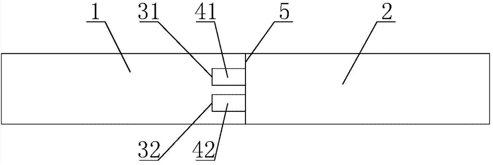
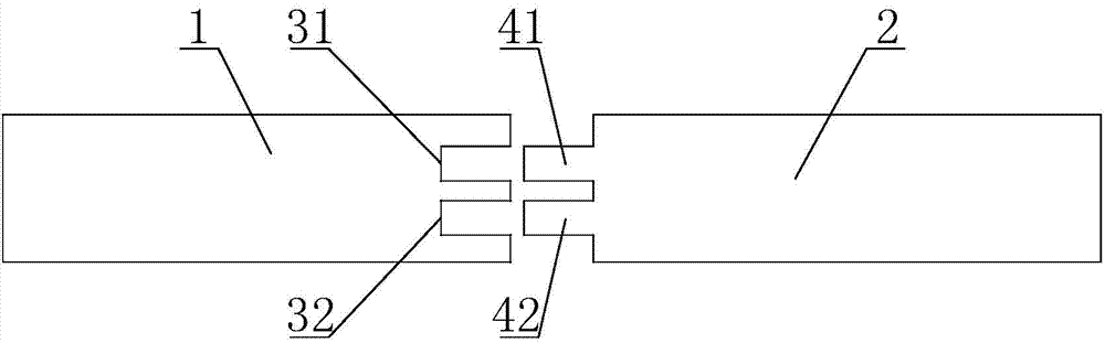
[0019] Such as figure 1 , figure 2 As shown, the seed crystal splicing method for single crystal silicon ingots of the embodiment of the present invention is used for directional solidification method of single crystal silicon ingots. The seed crystal layer is formed by closely arranging the seed crystal blocks. The splicing surface 5 between 1 and 2 is a plane perpendicular to the bottom of the crucible, and the seed crystal block 1 on one side of the splicing surface 5 is provided with elongated first rectangular grooves 31 and second rectangular grooves 32 from top to bottom. , The seed crystal block 2 on the other side of the splicing surface 5 has elongated first rectangular protrusions 41 and second rectangular protrusions 42 suitable for inserting into the first rectangular groove 31 and the second rectangular groove 32, respectively. The cross sections of the groove 31, the second rectangular groove 32, the first rectangular protrusion 41, and the second rectangular pr...


PUM


Abstract

The invention relates to a seed crystal splicing method for a monocrystalline-like silicon cast ingot. The monocrystalline-like silicon cast ingot comprises seed crystal blocks which are mutually spliced, wherein a splicing surface between adjacent seed crystal blocks is a plane perpendicular to the bottom of a crucible, two long-strip-shaped rectangular grooves are formed in each seed crystal block on one side of the splicing surface from top to bottom, two long-strip-shaped rectangular bumps which are suitable for being inserted into the rectangular grooves are arranged on each seed crystal block on the other side of the splicing surface, and after the adjacent seed crystal blocks are spliced, the rectangular bumps are inserted into corresponding rectangular grooves, and gaps among the splicing surfaces are less than 0.5mm. According to the monocrystalline-like silicon cast ingot disclosed by the invention, the rectangular bumps and the rectangular grooves which are matched mutually are arranged on the splicing surfaces of the seed crystal blocks to form mortise and tenon structures so as to ensure that the adhering degree of the seed crystal splicing surfaces can be improved; in a heating process, seed crystals on edges are heated to be expanded, the mortise and tenon structures are closer, the gaps become smaller, and the adjacent seed crystal blocks can be adhered more closely so as to prevent gap expansion caused by edge up-warping of the seed crystal blocks, so that crystal dislocation defects can be reduced to a highest extent, and the single crystal area proportion can be increased.

Description

Technical field [0001] The invention relates to a seed crystal splicing method for monocrystalline silicon ingots, and belongs to the field of silicon crystal manufacturing. Background technique [0002] In recent years, silicon single crystals and silicon polycrystals have been widely used in photovoltaic solar cells, liquid crystal displays and other fields. The current common manufacturing method for silicon-like single crystals is the directional solidification method, in which a cuboid seed crystal is laid on the bottom of a flat-bottomed crucible, and the seed crystals are arranged regularly to form a seed layer. The silicon material is placed in a flat bottom crucible and laid on the seed layer. Through the temperature control in the melting stage, after the silicon material is melted, the seed crystal gradually melts from the surface in contact with the silicon liquid, and then the directional heat dissipation is performed to achieve the directional growth of the silicon...

Claims


Application Information

Patent Timeline
Patent Type & Authority Applications(China)
IPC IPC(8): C30B11/14C30B28/06C30B29/06
Inventor 王强花国然李俊军邓洁
Owner NANTONG UNIVERSITY
Why Eureka
Try Eureka