A Design Method of Digital Marker in Test Layout

A technology of digital marking and virtual pattern, applied in electrical digital data processing, computing, special data processing applications, etc., can solve the problem of weakening the photolithography, etching process window, reducing the overall uniformity of the layer pattern, and not distinguishing the key layers of the design, etc. question

Active Publication Date: 2018-02-06
SEMICON MFG INT (SHANGHAI) CORP
View PDF3 Cites 0 Cited by
  • Summary
  • Abstract
  • Description
  • Claims
  • Application Information

AI Technical Summary

Problems solved by technology

like figure 1 As shown in the figure, the design of the digital marks described in the prior art is not distinguished from design critical layers (active area / gate / metal layer M1-M8, AA / GT / M1-M8) and non-critical layers (No. A top metal layer and / or a second top metal layer, TM1 / TM2) patterns, key layers and non-key layer digital marks are designed to directly define numbers with larger widths and lengths as digital marks, since the digital marks (numerical marker) has a large width and length and includes a lot of small convex corners (jog), so it will cause: key layer chemical mechanical polishing (CMP) process to form dishing, increase the key layer optical proximity effect Difficulty of correcting processing, weakening process windows of photolithography and etching; in addition, it will also reduce the overall uniformity of the layer pattern

Method used


Image

  • A Design Method of Digital Marker in Test Layout
  • A Design Method of Digital Marker in Test Layout
  • A Design Method of Digital Marker in Test Layout

Examples


Embodiment 1

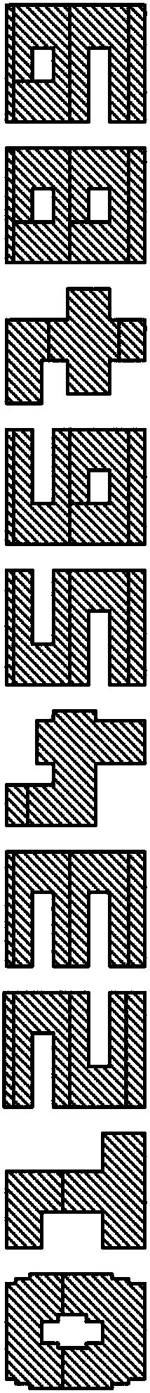
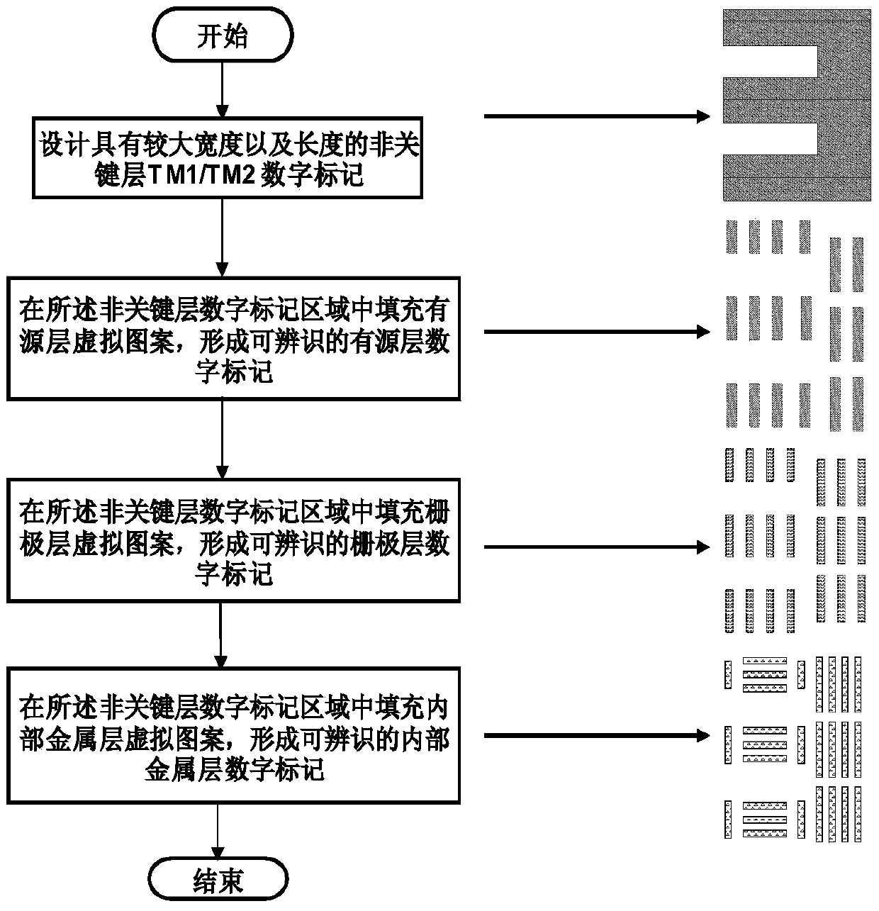
[0047] Attached below Figure 2-3 The method for forming the digital mark in this embodiment will be described in detail.

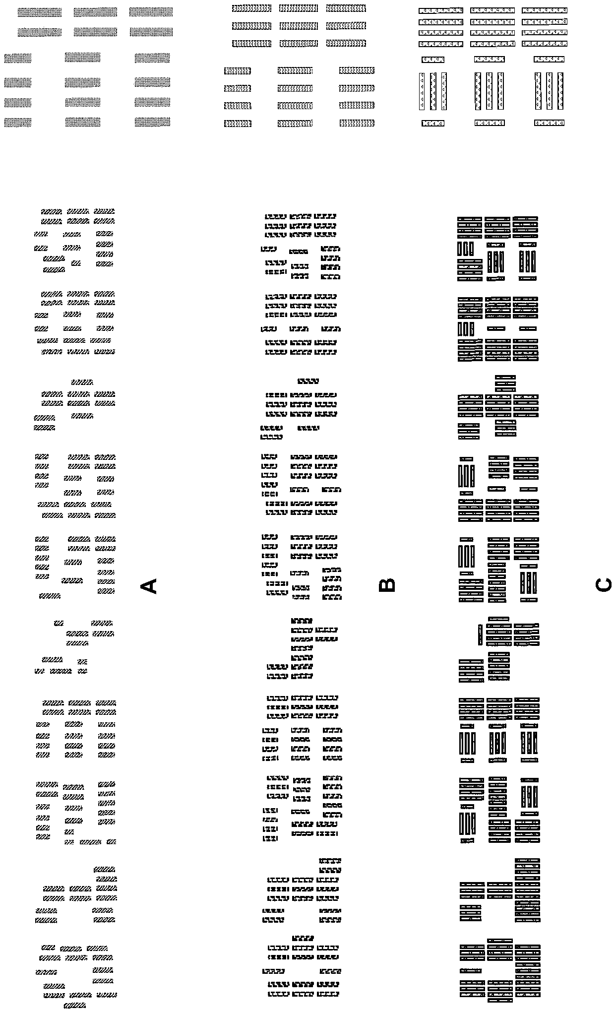
[0048] First, refer to figure 2 , in the present invention, in order to solve the problems caused by selecting a digital mark with a larger size on the key physical layer, a new method for forming a digital mark is provided, in which the non-critical physical layer (non-critical physical layers) and the key physical layer are designed differently, and digital marks with different key sizes are formed on different layers, so that the digital marks and the main pattern of the layer have a uniform key size.

[0049] For example in figure 2 Among them, digital marks with larger critical sizes are first formed in non-critical physical layers. The width and length of digital marks formed in non-critical physical layers are relatively large. Also in non-critical physical layers The standard circuit also has similar critical dimensions, so that a pattern wit...


PUM


Abstract

The present invention relates to a design method of a digital mark in a test layout, comprising: step (a) first directly defining a non-key layer digital mark, wherein the non-key layer digital mark has a relatively large length and width; step (b) Multiple virtual patterns of key layers are inserted into the non-key layer digital mark area to form recognizable key layer digital marks. In order to solve the problem in the prior art that the special pattern of the digital mark causes process defects, the invention provides a brand-new layout digital mark design method. The digital mark design method defines a digital mark through non-critical layers, and then fills the digital mark area with a universally existing dummy pattern to form a recognizable uniform digital mark including all physical layers. A more uniform pattern can be obtained throughout the layout by the described setting.

Description

technical field [0001] The invention relates to the field of semiconductors, and in particular, the invention relates to a design method for digital marks in a test layout. Background technique [0002] Integrated circuit manufacturing technology is a complicated process, and the technology is updated very quickly. A key parameter characterizing integrated circuit manufacturing technology is the minimum feature size, namely critical dimension (CD). With the continuous development of semiconductor technology, the critical dimensions of devices are getting smaller and smaller. It is precisely because of the reduction of critical dimensions that it is possible to set millions of devices on each chip. [0003] Design for Manufacturability (DFM) has become increasingly important in the semiconductor industry nano-design process methodology. The DFM refers to a unified description of the rules, tools and methods in chip design for the purpose of rapidly improving the production ...

Claims


Application Information

Patent Timeline
Patent Type & Authority Patents(China)
IPC IPC(8): G06F17/50
Inventor 樊强
Owner SEMICON MFG INT (SHANGHAI) CORP
Why Eureka
Try Eureka