Grid driving circuit, array substrate and display device

A gate drive circuit and drive unit technology, which is applied in the fields of gate drive circuits, array substrates and display devices, can solve the problems of easily causing horizontal stripes and obvious horizontal stripes, and achieve the effect of improving quality

Active Publication Date: 2015-07-15
BOE TECH GRP CO LTD +1
View PDF7 Cites 8 Cited by
  • Summary
  • Abstract
  • Description
  • Claims
  • Application Information

AI Technical Summary

Problems solved by technology

[0005] However, the following problems are found in practical applications by adopting the above-mentioned 2-point driving method: such as image 3 As shown, the color of the odd-numbered

Method used


Image

  • Grid driving circuit, array substrate and display device
  • Grid driving circuit, array substrate and display device
  • Grid driving circuit, array substrate and display device

Examples


Embodiment Construction

[0028] In order for those skilled in the art to better understand the technical solutions of the present invention, the gate drive circuit, array substrate and display device provided by the present invention will be described in detail below with reference to the accompanying drawings.

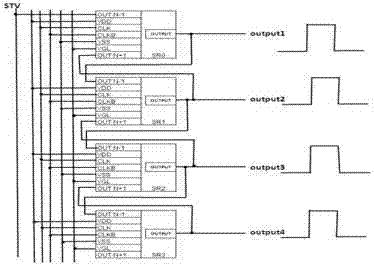
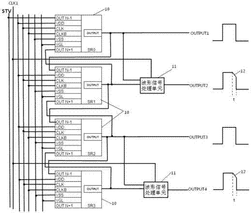
[0029] Figure 4 A schematic circuit diagram of a gate driving circuit provided by an embodiment of the present invention. see Figure 4 , the gate drive circuit provided in this embodiment is used to sequentially input scan signals to a plurality of gate lines (not shown in the figure) row by row, which includes a plurality of cascaded drive units 10 corresponding to the gate lines one by one and a waveform processing unit 11. Wherein, the drive unit 10 is similar to the prior art, and will not be described in detail here; the waveform processing unit 11 is arranged between the output end of the drive unit 10 corresponding to the gate line of the even row and the gate line, for the grid li...


PUM


Abstract

The invention provides a grid driving circuit, an array substrate and a display device. The grid driving circuit is used for sequentially inputting scanning signals to a plurality of grid lines line-by-line, the grid driving circuit comprises a plurality of driving units and waveform processing units which are arranged in a cascade connection mode and in one-to-one correspondence with the grid lines, the waveform processing units are arranged between the output ends of the driving units corresponding to the grid lines arranged on the even number lines and the grid lines, the waveform processing units are used for processing the waveforms of the output signals of the driving units corresponding to the grid lines into angle cutting weaves and take signals with the waveforms being angle cutting weaves as scanning signals to input the signals into the grid lines. The grid driving circuit can achieve equal charging voltages of sub-pixels of the even number lines and the sub-pixels of the odd number lines, and therefore the problem that cross stripes occur due to the fact that the grid driving circuit is driven by a two-point mode is solved, and therefore the quality of the array substrate and the display device is improved.

Description

technical field [0001] The invention belongs to the technical field of liquid crystal display, and in particular relates to a gate drive circuit, an array substrate and a display device. Background technique [0002] GOA (Gate Driver On Array) technology concentrates the gate switching circuit on the array substrate, because it not only saves the part of the gate driver integrated circuit, but also saves the process of binding the integrated circuit, therefore, It is widely used in thin film transistor liquid crystal display (Thin Film Transistor Liquid Crystal Display, referred to as TFT LCD). [0003] figure 1 Circuit diagram for the existing GOA unit. see figure 1 , the GOA circuit has a plurality of GOA units, and each GOA unit has a positive clock input signal CLK, a reverse clock input signal CLKB, a low voltage signal VSS, and a high voltage signal VDD, wherein each GOA unit also has an input terminal INPUT , output terminal OUTPUT, reset terminal RESET, and the o...

Claims


Application Information

Patent Timeline
IPC IPC(8): G09G3/36
Inventor 江定荣李兴华贺伟
Owner BOE TECH GRP CO LTD
Why Eureka
Try Eureka