Supercharge Your Innovation With Domain-Expert AI Agents!

Pixel bias circuit and control method for oversized-area-array CMOS (complementary metal-oxide-semiconductor transistor) image sensor

A technology of image sensor and bias circuit, which is applied in the direction of image communication, television, electrical components, etc., and can solve the problems of poor output current consistency and large current difference

Active Publication Date: 2015-07-22
NO 771 INST OF NO 9 RES INST CHINA AEROSPACE SCI & TECH
View PDF7 Cites 0 Cited by
  • Summary
  • Abstract
  • Description
  • Claims
  • Application Information

AI Technical Summary

Problems solved by technology

If the pixel bias circuit is used for a large area array pixel such as N is much greater than 64, the parasitic resistance 299-352 of the ground wire will produce a voltage drop, which will cause a large difference in the gate-source voltage of the common source transistor 235-298, resulting in output Each current I OUT The difference is large, and the output current consistency of each channel is poor

Method used


Image

  • Pixel bias circuit and control method for oversized-area-array CMOS (complementary metal-oxide-semiconductor transistor) image sensor
  • Pixel bias circuit and control method for oversized-area-array CMOS (complementary metal-oxide-semiconductor transistor) image sensor
  • Pixel bias circuit and control method for oversized-area-array CMOS (complementary metal-oxide-semiconductor transistor) image sensor

Examples


Embodiment Construction

[0036] The present invention will be further described below in conjunction with embodiment.

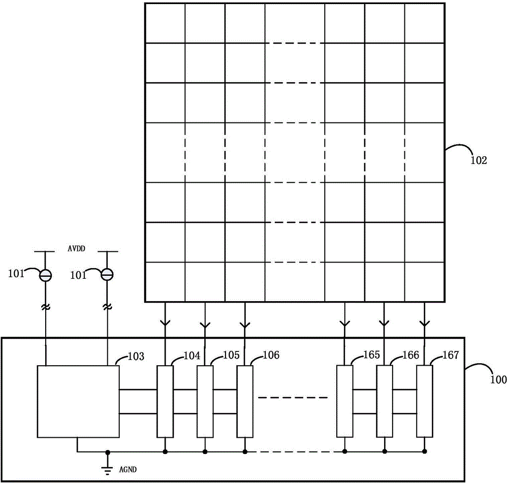
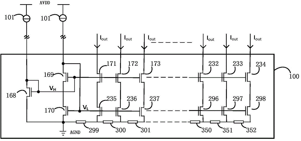
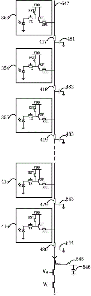
[0037] see Figure 4 , the pixel bias circuit of the present invention includes a first-stage bias current generating circuit 548, a second-stage bias current generating circuit 549, and a third-stage bias current generating circuit 550 connected in sequence, and the first-stage bias current generates The circuit 548 is connected with two current sources 101, and the first-stage bias current generating circuit 548, the second-stage bias current generating circuit 549 and the third-stage bias current generating circuit 550 all use two equivalent currents Input high-swing cascode structure, the first-stage bias current generating circuit 548 and the second-stage bias current generating circuit 549 both adopt PMOS output, and the third-stage bias current generating circuit 550 adopts NMOS output; The first-stage bias current generating circuit 548, the second-stage bias current generat...


PUM


Abstract

The invention discloses a pixel bias circuit and a control method for an oversized-area-array CMOS (complementary metal-oxide-semiconductor transistor) image sensor and aims to lower influences of ground wire parasitic resistance on pixel bias current precision and consistency and influences of pixel leakage current and line parasitic capacitance on row FPN (fixed pattern noise). The technical scheme includes that the pixel bias circuit comprises a first-stage bias current generating circuit, a second-stage bias current generating circuit and a third-stage bias current generating circuit which are connected in sequence, each of the first-stage bias current generating circuit, the second-stage bias current generating circuit and the third-stage bias current generating circuit is of a high-swing cascade structure with two circuits of equivalent current input, a voltage transmission mode is adopted in each of the first-stage bias current generating circuit, the second-stage bias current generating circuit and the third-stage bias current generating circuit, and a current transmission mode is adopted between every two of the first-stage bias current generating circuit, the second-stage bias current generating circuit and the third-stage bias current generating circuit.

Description

technical field [0001] The invention belongs to the technical field of CMOS image sensors, and in particular relates to a pixel bias circuit and a control method for super large area array CMOS image sensors. Background technique [0002] In the mainstream CMOS image sensor, the pixel structure mainly uses the source follower as the output device, and the pixel bias circuit is used as the current source load of the source follower to provide the pixel array with high-precision and high-consistency column current. , to ensure that the pixel array works normally and stably. In small-scale CMOS image sensors, the highest accuracy reported so far is the voltage path mode cascode structure pixel bias circuit. However, in CMOS image sensors with tens of millions of pixels and above, due to the increase in the power consumption of the pixel bias circuit and the increase in the parasitic resistance of the ground wire, the channel length modulation effect seriously affects the relat...

Claims


Application Information

Patent Timeline
IPC IPC(8): H04N5/374H04N5/357
Inventor 李栋刘文平郭仲杰何杰肖筱刘理想
Owner NO 771 INST OF NO 9 RES INST CHINA AEROSPACE SCI & TECH
Features
  • R&D
  • Intellectual Property
  • Life Sciences
  • Materials
  • Tech Scout
  • Unparalleled Data Quality
  • Higher Quality Content
  • 60% Fewer Hallucinations
Learn More