Check patentability & draft patents in minutes with Patsnap Eureka AI!

Array substrate, manufacturing method of array substrate and display device

A technology of an array substrate and a manufacturing method, which is applied in the field of display, can solve problems such as poor display, poor overlap, and affecting the aperture ratio of a display device, and achieve the effects of reducing the probability of poor display, increasing the aperture ratio, and optimizing connection conditions

Inactive Publication Date: 2015-08-12
HEFEI BOE OPTOELECTRONICS TECH +1
View PDF4 Cites 16 Cited by
  • Summary
  • Abstract
  • Description
  • Claims
  • Application Information

AI Technical Summary

Problems solved by technology

[0004] Existing ADS array substrates generally use the gate metal layer to make the common electrode lines, use the transparent conductive layer to make the common electrodes, and connect the common electrode lines and the common electrodes through the vias set in the pixel area, due to the number of vias More, so it will affect the aperture ratio of the display device; and because the common electrode line and the common electrode are overlapped together through the via hole, there is also a risk of poor bonding at the via hole, resulting in an increase in the probability of poor display

Method used


Image

  • Array substrate, manufacturing method of array substrate and display device
  • Array substrate, manufacturing method of array substrate and display device
  • Array substrate, manufacturing method of array substrate and display device

Examples


Embodiment 1

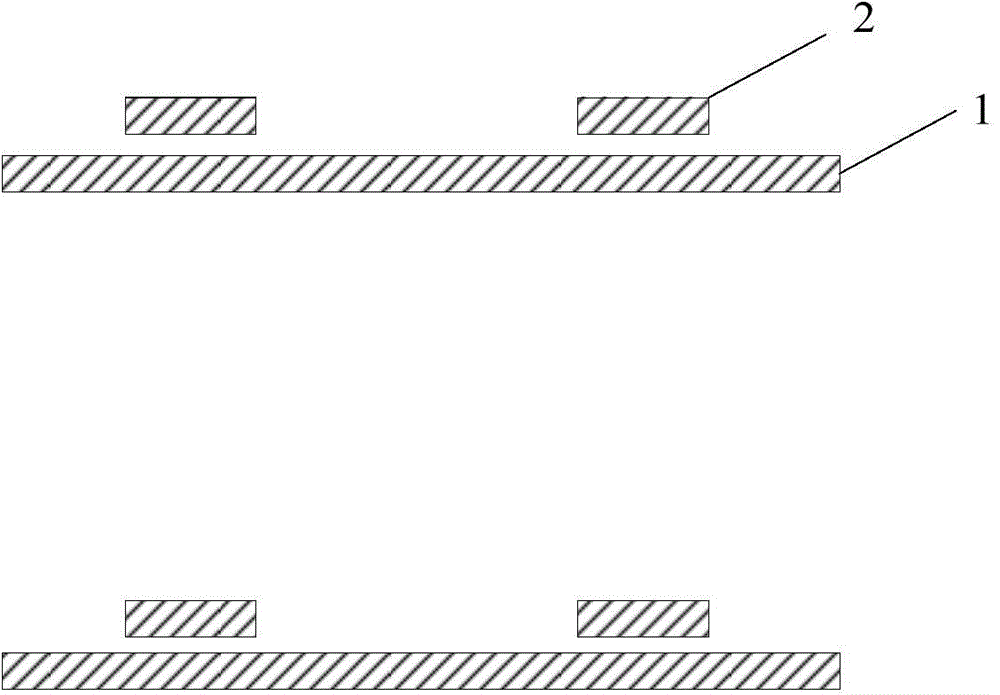
[0044] This embodiment provides an array substrate, including a gate electrode, a gate line, a gate insulating layer, a source electrode, a drain electrode, a data line, a common electrode and a common electrode line formed on the base substrate, wherein the common electrode The wire is directly connected to the common electrode.

[0045] The common electrodes of the array substrate in this embodiment are directly connected to the common electrode lines instead of through via holes, so there is no need to provide via holes for connecting the common electrode lines and common electrodes, which can improve the aperture ratio of the display device, and the common electrode The direct connection with the common electrode line can optimize the connection between the common electrode and the common electrode line, and reduce the probability of poor display.

[0046] In a specific embodiment, the common electrode line and the source electrode, the drain electrode, and the data line a...

Embodiment 2

[0053] This embodiment provides a display device, including the above-mentioned array substrate. The display device can be any product or component with a display function such as a liquid crystal panel, a liquid crystal TV, a liquid crystal display, a digital photo frame, a mobile phone, a tablet computer, a navigator, and an electronic paper.

Embodiment 3

[0055] This embodiment provides a method for fabricating an array substrate, the array substrate comprising a gate electrode, a gate line, a gate insulating layer, a source electrode, a drain electrode, a data line, a common electrode and a common electrode line formed on a base substrate, Wherein, the preparation method includes:

[0056] A directly connected common electrode line and common electrode are formed.

[0057] The common electrodes formed in this embodiment are directly connected to the common electrode lines, rather than through via holes, so there is no need to provide via holes for connecting the common electrode lines and the common electrodes, and the aperture ratio of the display device can be improved. The direct connection of the common electrode lines can optimize the connection between the common electrodes and the common electrode lines and reduce the probability of poor display.

[0058] In a specific embodiment, the manufacturing method includes:

...


PUM


Abstract

The invention provides an array substrate, a manufacturing method of the array substrate and a display device, and belongs to the technical field of display. The array substrate comprises a gate electrode, gate lines, a gate insulating layer, a source electrode, a drain electrode, data lines, a common electrode and common electrode lines, wherein the common electrode lines are directly connected with the common electrode. According to the technical scheme provided by the invention, the aperture ratio of the display device can be improved, a connection condition of the common electrode and the common electrode lines can be optimized at the same time, and the occurrence probability of poor display is reduced.

Description

technical field [0001] The present invention relates to the field of display technology, in particular to an array substrate, a manufacturing method thereof, and a display device. Background technique [0002] With the progress of the TFT (Thin Film Transistor, thin film transistor) industry and the improvement of technology, AD-ADS (ADvanced Super Dimension Switch, Advanced Super Dimension Switch, referred to as ADS) wide viewing angle technology has been applied to more and more products Among them, including mobile phones, digital cameras, tablet computers, notebook computers, and LCD TVs, etc., their excellent display characteristics have been praised by more and more users, and their market competitiveness is very strong. [0003] ADS technology is to form a multi-dimensional electric field through the electric field generated by the edge of the slit electrode in the same plane and the electric field generated between the slit electrode layer and the plate electrode lay...

Claims


Application Information

Patent Timeline
IPC IPC(8): H01L21/768H01L21/84H01L23/52H01L27/12
CPCH01L21/768H01L21/84H01L23/52H01L27/1214G02F1/136286G02F2201/40G02F1/134372H01L27/124H01L27/1259
Inventor 陈传宝王炎
Owner HEFEI BOE OPTOELECTRONICS TECH
Features
  • R&D
  • Intellectual Property
  • Life Sciences
  • Materials
  • Tech Scout
  • Unparalleled Data Quality
  • Higher Quality Content
  • 60% Fewer Hallucinations
Learn More