Manufacture method of circuit board

A production method and circuit board technology, applied in the directions of printed circuit manufacturing, printed circuits, electrical components, etc., can solve problems such as short circuit scrapping of circuit boards, and achieve the effect of improving the pass rate and realizing metallization

Active Publication Date: 2015-08-12
GCI SCI & TECH
View PDF4 Cites 7 Cited by
  • Summary
  • Abstract
  • Description
  • Claims
  • Application Information

AI Technical Summary

Problems solved by technology

[0004] However, the above process can only produce simple blind slot circuit boards. When making blind slot side wall metallized circuit boards, copper plating on the blind slot side walls will inevitably sink copper on the entire circuit board, resulting in blind slot side The circuit pattern on the wall and the bottom of the blind slot is the same circuit network, which causes the circuit board to be short-circuited and scrapped

Method used


Image

  • Manufacture method of circuit board
  • Manufacture method of circuit board
  • Manufacture method of circuit board

Examples


Embodiment Construction

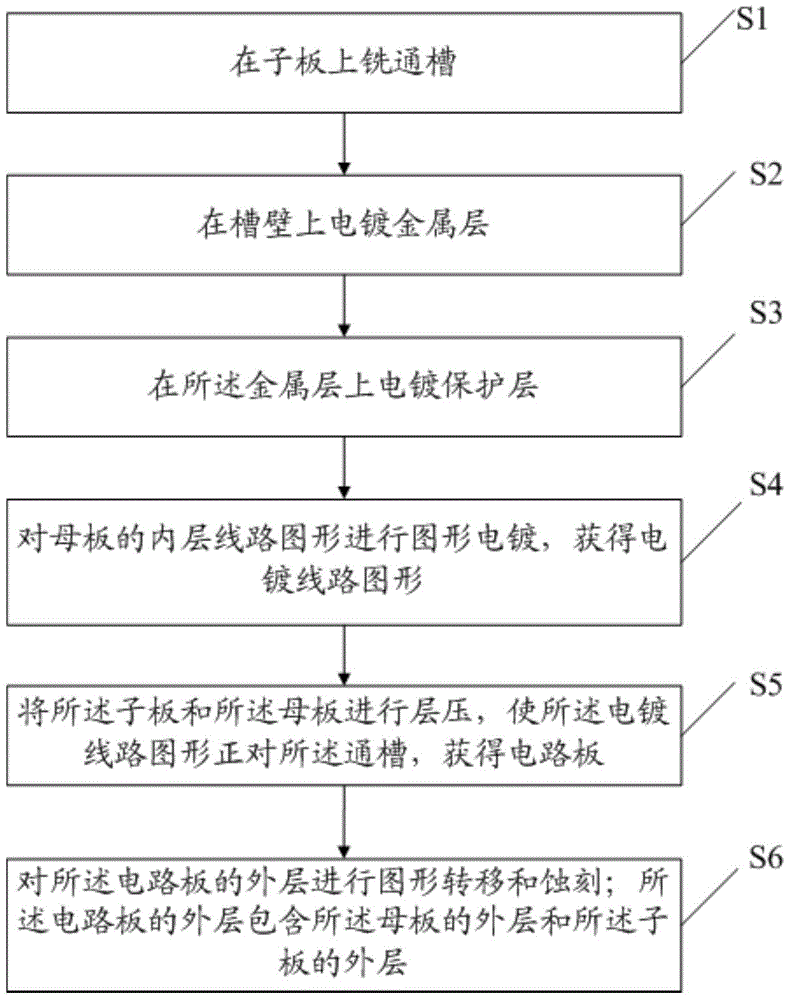
[0056] The following will clearly and completely describe the technical solutions in the embodiments of the present invention with reference to the accompanying drawings in the embodiments of the present invention. Obviously, the described embodiments are only some, not all, embodiments of the present invention. Based on the embodiments of the present invention, all other embodiments obtained by persons of ordinary skill in the art without creative efforts fall within the protection scope of the present invention.

[0057] see figure 1 , is a schematic flow diagram of an embodiment of the method for manufacturing a circuit board provided by the present invention, including:

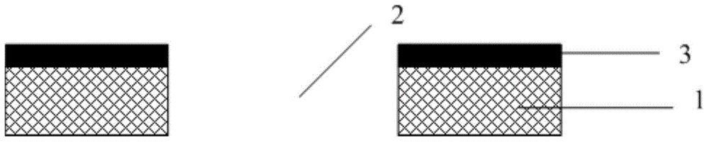
[0058] S1, milling slots on the daughter board;

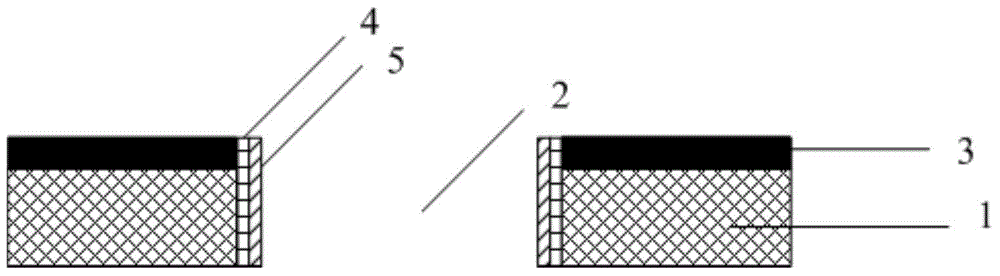
[0059] S2, electroplating a metal layer on the tank wall;

[0060] S3. Plating a protective layer on the metal layer;

[0061] S4. Perform pattern electroplating on the inner layer circuit pattern of the motherboard to obtain the electroplating circuit ...


PUM


Abstract

The invention discloses a manufacture method of a circuit board. The method comprises the following steps: milling a through groove in a daughter board; electroplating a metal layer on the wall of the groove; electroplating a protective layer on the metal layer; performing pattern electroplating on the internal-layer line patterns of a motherboard to obtain electroplating line patterns; laminating the daughter board and the motherboard to enable the electroplating line patterns to be right opposite to the through groove, and obtaining the circuit board; and performing pattern transferring and etching on the external layer of the circuit board, wherein the external layer of the circuit board comprises the external layer of the motherboard and the external layer of the daughter board. By using the method provided by the embodiment of the invention, metallization of the groove wall of the circuit board can be realized, and the qualified rate of the circuit board is improved.

Description

technical field [0001] The invention relates to the technical field of circuit board manufacturing technology, in particular to a method for manufacturing a circuit board. Background technique [0002] With the rapid development of the communication and telecommunication industries, electronic products are increasingly trending towards miniaturization, high integration and high frequency. Some electronic terminal products introduce blind slot design for installing components or fixing products. [0003] At present, the specific process of making blind slots in the circuit board manufacturing industry is: milling through the prepreg and daughter board → making the inner circuit pattern of the mother board → pressing the daughter board, prepreg and mother board into a circuit board → making the outer layer of the circuit board Line graphics. [0004] However, the above process can only produce simple blind slot circuit boards. When making blind slot side wall metallized circ...

Claims


Application Information

Patent Timeline
IPC IPC(8): H05K3/42
CPCH05K3/424H05K2203/143
Inventor 胡伦洪关志锋唐有军
Owner GCI SCI & TECH
Why Eureka
Try Eureka