Supercharge Your Innovation With Domain-Expert AI Agents!

Pixel circuit, display device and display driving method

A pixel circuit and capacitor technology, which is applied in the field of pixel circuits, display devices and display drivers, can solve problems such as uneven display, and achieve the effect of compensating for different threshold voltages and offsetting threshold voltages

Active Publication Date: 2015-08-26
PEKING UNIV SHENZHEN GRADUATE SCHOOL
View PDF5 Cites 31 Cited by
  • Summary
  • Abstract
  • Description
  • Claims
  • Application Information

AI Technical Summary

Problems solved by technology

Although this circuit structure is simple, when the threshold voltage V of the driving transistor 11 TH Drift, OLED14 degradation over time causing V OLED When the increase or use of polysilicon material causes the threshold voltage of the driving transistors to be uneven across the panel, the current flowing through the OLED14 will change with time or spatial position, resulting in uneven display

Method used


Image

  • Pixel circuit, display device and display driving method
  • Pixel circuit, display device and display driving method
  • Pixel circuit, display device and display driving method

Examples


Embodiment 1

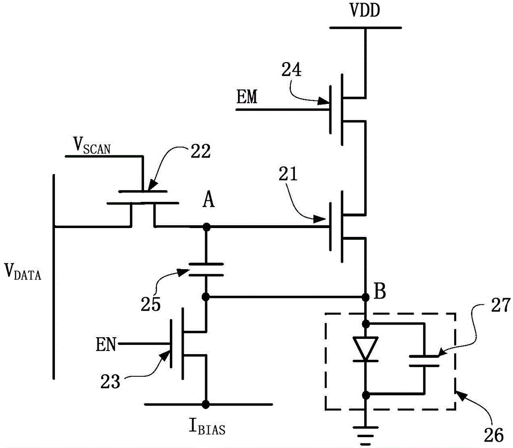
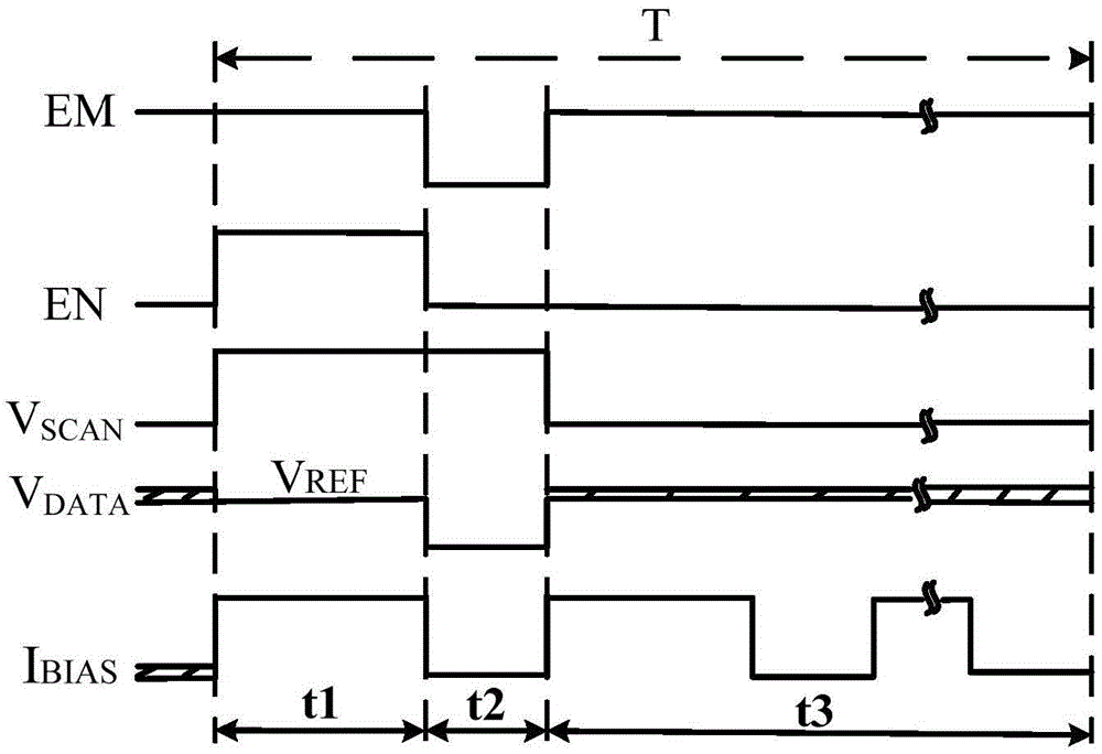
[0048] Please refer to figure 2 , the pixel circuit in this embodiment includes a first transistor 21 , a second transistor 22 , a third transistor 23 , a fourth transistor 24 , a first capacitor 25 , a second capacitor 27 and a light emitting device 26 .

[0049] The fourth transistor 24, the first transistor 21 and the light emitting device 26 are serially connected in series between the first voltage source VDD and the ground. The control electrode of the fourth transistor 24 is connected to the third scan control signal line, and is turned on or off under the control of the third scan control signal EM.

[0050] The control electrode of the second transistor 22 is coupled to the first scan control signal line for receiving the first scan control signal V SCAN , the first electrode of the second transistor 22 is coupled to the data signal line for receiving data information on the data signal line, and the second electrode of the second transistor 22 is coupled to the con...

Embodiment 2

[0080] Such as Figure 5 As shown, the main difference from Embodiment 1 is that a fifth transistor 28 is added, and the first scanning control signal line of the previous row of pixel circuits is used as the second scanning control signal line of the current row to control the third transistor 23 of the current row. and the fifth transistor 28, which can reduce a set of scan control signal generating circuits and simplify peripheral circuits.

[0081] Devices whose connection relationship does not change in the circuit will not be repeated here. The control electrode of the third transistor 23 is connected to the first scanning control signal line of the previous row, the first electrode is connected to the bias current signal line, and the second electrode is coupled to the second node B for responding to the first scan control signal line of the previous row. The scanning control signal provides bias current information for the first transistor 21 in the first threshold vo...

Embodiment 3

[0093] Please refer to Figure 8 , the pixel circuit in this embodiment includes a first transistor 61 , a second transistor 62 , a third transistor 63 , a fourth transistor 64 , a first capacitor 65 , a second capacitor 66 and a light emitting device 67 .

[0094] The fourth transistor 64 , the first transistor 61 and the light emitting device 67 are sequentially connected in series between the first voltage source VDD and the ground. The control electrode of the fourth transistor 64 is connected to the third scanning control signal line, and is turned on or off under the control of the third scanning control signal. In this embodiment, V SCAN Both the first scan control signal and the third scan control signal are used as the first scan control signal in this embodiment.

[0095] The control electrode of the second transistor 62 is coupled to the first scan control signal line for receiving the first scan control signal V SCAN , the first electrode of the second transistor...


PUM


Abstract

The application discloses a pixel circuit, a display device and a display driving method. The pixel circuit of the application generates the information relevant with a first threshold voltage of a driving transistor in a current bias manner, generates the reference voltages relevant with the first threshold voltage and the gray information at the two ends of a first capacitor by the voltage division of the first capacitor and a second capacitor, and during an luminescence process, enables the reference voltages at the two ends of the first capacitor to be constant, so that a driving current flowing through a light-emitting device is irrelevant with the first threshold voltage of the driving transistor and a second threshold voltage of the light-emitting device. The pixel circuit can compensate the threshold voltage shift of the driving transistor and the light-emitting device, and also can compensate the uneven display problem caused by the different driving transistor threshold voltages of a display panel.

Description

technical field [0001] The present application relates to the field of display devices, in particular to a pixel circuit, a display device and a display driving method. Background technique [0002] Organic Light-Emitting Diode (OLED: Organic Light-Emitting Diode) display has been widely studied in recent years due to its advantages of high brightness, high luminous efficiency, wide viewing angle, low power consumption, and low manufacturing cost, and has been rapidly applied to a new generation of displays. device. OLED display can be divided into PMOLED (Passive Matrix OLED: Passive Matrix OLED) and AMOLED (Active Matrix OLED: Active Matrix OLED) according to the pixel driving method. Although PMOLED has low manufacturing cost, it has crosstalk and requires a large driving current, so it has disadvantages such as short service life and high power consumption, and cannot meet the display requirements of large area and high resolution. In contrast, AMOLED avoids problems s...

Claims


Application Information

Patent Timeline
IPC IPC(8): G09G3/32
Inventor 张盛东王翠翠冷传利
Owner PEKING UNIV SHENZHEN GRADUATE SCHOOL
Features
  • R&D
  • Intellectual Property
  • Life Sciences
  • Materials
  • Tech Scout
  • Unparalleled Data Quality
  • Higher Quality Content
  • 60% Fewer Hallucinations
Learn More