Yield enhancement (YE) on-line detection management and control method

A detection tube and detection station technology, applied in the direction of semiconductor/solid-state device testing/measurement, etc., can solve the problems of product skipping, low product priority, limited production capacity, etc., and achieve the effect of improving detection efficiency and reducing defect risk.

Active Publication Date: 2015-08-26
SEMICON MFG INT (SHANGHAI) CORP
View PDF4 Cites 16 Cited by
  • Summary
  • Abstract
  • Description
  • Claims
  • Application Information

AI Technical Summary

Problems solved by technology

[0006] However, the production capacity of YE online defect inspection machines is limited. The more measurements are made, the relative prolongation of the production cycle of semiconductor products will be caused, which will have a negative impact on the production of semiconductor products.
At the same time, at present, the defect risk of production equipment can only be judged based on experience, while inspection dispatching relies on the production plan level of the manufacturing department to arrange online inspection or skip inspection, and then it is easy to happen that products that need priority inspection are skipped, or products that require priority inspection The product is assigned a lower priority, and the defect risk of the production machine cannot be effectively controlled
[0007] Therefore, how to more efficiently allocate YE inspection sites, inspection frequency, inspection priority, etc. under the limited YE online defect inspection capacity is a big challenge for YE online defect inspection

Method used


Image

  • Yield enhancement (YE) on-line detection management and control method
  • Yield enhancement (YE) on-line detection management and control method

Examples


Embodiment Construction

[0034] In order to make the purpose, technical solution and advantages of the present invention more clear, the present invention will be further described in detail below with reference to the accompanying drawings and examples.
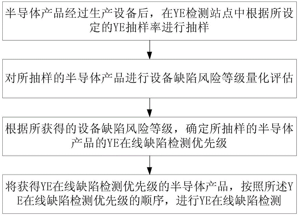
[0035] The main core idea of ​​the present invention is to determine the equipment defect risk level according to the production equipment characteristics and historical defect statistics, and according to the equipment defect risk level, combined with YE online defect detection, determine the YE sampling rate and YE online defect detection priority to achieve optimization The purpose of defect detection sampling in YE online defect detection is to improve the detection efficiency of YE online detection machines and reduce the defect risk of production machines.

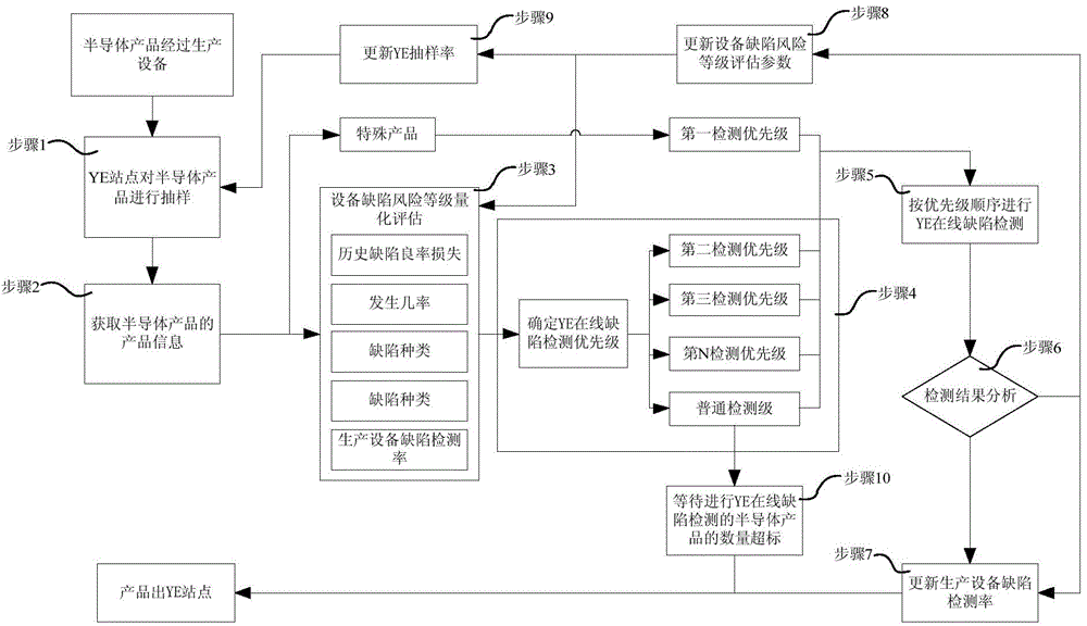
[0036] According to this idea, if figure 1 As shown, the YE online detection and control method embodiment of the present invention includes:

[0037] After semiconductor products pass th...


PUM


Abstract

The present invention discloses a YE on-line detection management and control method. The method comprises the steps of sampling the semiconductor products passing the production equipment according to a set YE sampling rate, determining the equipment defect risk grade by an equipment defect risk grade quantification assessment means, deciding the YE on-line defect detection priorities of the sampled semiconductor products according to the equipment defect risk grade to carry out the subsequent equipment defect detection, then adjusting a YE sampling rate, the YE on-line defect detection priorities, an equipment defect risk grade quantification assessment parameter, a production equipment defect detection rate according to the good and bad equipment defect detection results. The YE on-line detection management and control method of the present invention optimizes the YE sampling rate, the YE on-line defect detection priorities, the equipment defect risk grade quantification assessment parameter and the production equipment defect detection rate in the YE on-line defect detection according to each time of detection result, thereby improving the detection efficiency of a YE on-line detection board, and reducing the defect risk of a production board.

Description

technical field [0001] The invention relates to semiconductor manufacturing detection technology, in particular to a method for on-line detection management and control in the semiconductor manufacturing process. Background technique [0002] In the production process of semiconductor integrated circuits, semiconductor products need to go through hundreds of processes from raw materials to final products, and all the processes that the wafer goes through constitute the entire process flow. [0003] Because semiconductor integrated circuits are high-precision products, the critical dimension (CD, Critical Dimension) is on the order of submicron to nanometer. Therefore, in the production line of semiconductor production, a large number of detection methods will be used in the production process to track whether various parameters in the production process of semiconductor products meet the design requirements, so as to ensure the product quality of semiconductor integrated cir...

Claims


Application Information

Patent Timeline
Patent Type & Authority Applications(China)
IPC IPC(8): H01L21/66
Inventor 方三军杨健陈思安朱瑜杰
Owner SEMICON MFG INT (SHANGHAI) CORP
Why Eureka
Try Eureka