
A semi-floating gate device with a drain region embedded in an inversion layer and its manufacturing method

A technology of semi-floating gate devices and inversion layers, which is applied in semiconductor devices, electrical solid state devices, electrical components, etc., can solve the problems of reduced device storage speed, large leakage, and low occurrence rate of inter-band tunneling, etc. Bipolar effect, increased manufacturing cost, and increased manufacturing difficulty

Active Publication Date: 2018-10-16
SHANGHAI INTEGRATED CIRCUIT RES & DEV CENT +1
View PDF5 Cites 0 Cited by
  • Summary
  • Abstract
  • Description
  • Claims
  • Application Information

AI Technical Summary

Problems solved by technology

[0011] 1) The incidence of inter-band tunneling embedded in TFETs is not high, resulting in a reduction in device storage speed
2) When inter-band tunneling occurs, the leakage current is large due to the bipolar effect of the embedded TFET

Method used


Image

  • A semi-floating gate device with a drain region embedded in an inversion layer and its manufacturing method
  • A semi-floating gate device with a drain region embedded in an inversion layer and its manufacturing method
  • A semi-floating gate device with a drain region embedded in an inversion layer and its manufacturing method

Examples


Embodiment Construction

[0045] In order to make the content of the present invention clearer and easier to understand, the content of the present invention will be further described below in conjunction with the accompanying drawings. Of course, the present invention is not limited to this specific embodiment, and general replacements known to those skilled in the art are also covered within the protection scope of the present invention.

[0046] Secondly, the present invention is described in detail by means of schematic diagrams. When describing the examples of the present invention in detail, for the convenience of explanation, the schematic diagrams are not partially enlarged according to the general scale, which should not be used as a limitation of the present invention.

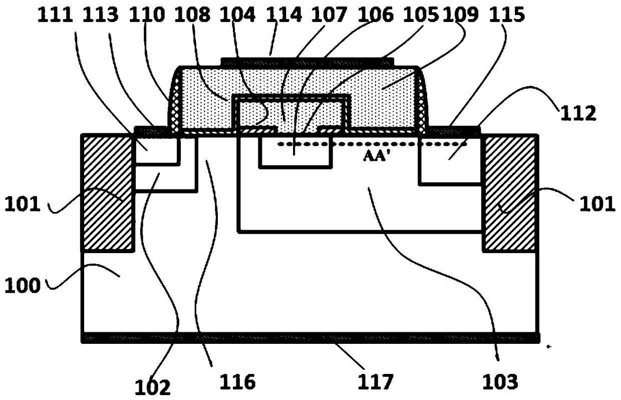
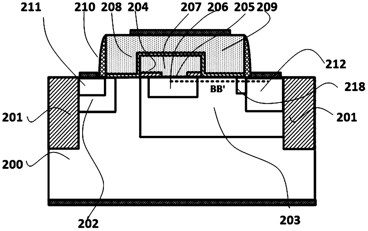
[0047] The semi-floating gate device in which the drain region is embedded in the inversion layer proposed by the present invention includes: a semiconductor substrate, an active region and a field oxygen region located on the...


PUM


Abstract

The invention proposes a semi-floating gate device with a drain region embedded in an inversion layer and a manufacturing method thereof. The device includes: a semiconductor substrate, a planar channel region located in the active region of the semiconductor substrate, and source regions and The drain area has a first insulating layer with a floating gate opening on the surface of the drain area, covering the floating gate opening and the floating gate of the first insulating layer. There is a diffusion area in the drain area below the floating gate opening, and the second insulating layer covers the entire floating gate. The control gate is located above the second insulating layer on part of the surface of the source and drain regions and the entire planar channel area, and there are also metal connections to lead out the gate, source, drain and substrate of the device. The characteristic is that at the drain In the region, an inversion layer is embedded in the drain region between the channel region and the heavily doped drain region of the embedded tunneling transistor below the control gate. The present invention optimizes the doping concentration gradient distribution between the channel and the drain region of the embedded tunneling lattice tube by adding an embedded inversion layer, improves the occurrence rate of inter-band tunneling, improves the read and write speed of the semi-floating gate device, and reduces the device cost. Leakage.

Description

technical field [0001] The invention belongs to the technical field of semiconductor memory. The invention relates to a semi-floating gate device (Semi-Floating Gate transistor) using a drain region embedded in an inversion layer and a manufacturing method. Background technique [0002] Memory is one of the basic core chips of electronic products. It is widely used in various electronic products, including mobile phones, mobile handheld products, etc. Among them, non-volatile memory (Nonvolatile memory, NVM) has the characteristics of long-term data storage in case of power failure. . The mainstream structure of the non-volatile memory in the prior art is the floating gate transistor. [0003] In order to further improve the performance of the floating gate semiconductor memory, the concept of a semi-floating gate transistor (Semi-Floating Gate Transistor, SFGT) is proposed. A window is opened between the drain region of the device and the insulating layer of the floating ...

Claims


Application Information

Patent Timeline
Patent Type & Authority Patents(China)
IPC IPC(8): H01L27/11521H10B41/30H10B69/00
Inventor 庄翔王全孙德明
Owner SHANGHAI INTEGRATED CIRCUIT RES & DEV CENT
Features
  • Generate Ideas
  • Intellectual Property
  • Life Sciences
  • Materials
  • Tech Scout
  • Unparalleled Data Quality
  • Higher Quality Content
  • 60% Fewer Hallucinations
Learn More