

Manufacturing method of circular magnetic random access memory cell structure
A technology of random access memory and manufacturing method, which is applied in the manufacture/processing of electromagnetic devices, photolithographic process of patterned surface, instruments, etc., and can solve the problem of large MRAM unit size, low memory density, and inability to apply magnetic random access Memory and other issues, to achieve cost savings, less sidewall process and etching process steps
- Summary
- Abstract
- Description
- Claims
- Application Information
AI Technical Summary
Problems solved by technology
Method used
Image

Examples
Embodiment Construction
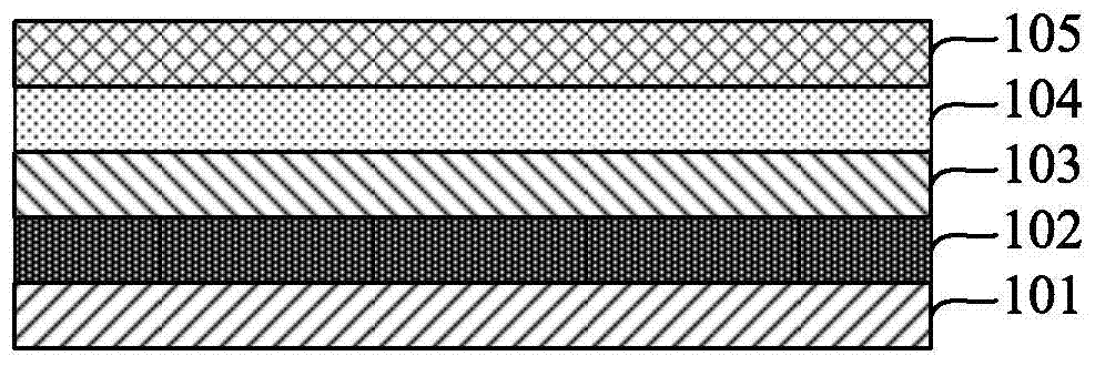
[0032] The hard mask layer (105) is silicon nitride, silicon dioxide, nitrogen-free oxycarbide film (NFC), nitrogen-doped silicon carbide (NDC), black diamond (BD), or any reasonable combination thereof.
[0033] In the present invention, after the bottom electrode / magnetic tunnel junction / top electrode (BE / MTJ / TE) layers are deposited on the semiconductor substrate, a hard mask layer is deposited. The hard mask layer can be insulating materials such as silicon nitride, silicon dioxide, nitrogen-free carbon oxide film (NFC), nitrogen-doped silicon carbide (NDC), black diamond (BD), or any reasonable combination. After the positive photoresist is spin-coated and exposed, the wafer is developed twice to complete the ring-shaped pattern. The first development is a positive tone aqueous developer (positive tone aqueous developer), and the second development is a negative organic developer. liquid (negative tone organic developer). The positive aqueous developer detects the solub...
PUM
 Abstract
Description
Claims
Application Information