Post-processing method and use method of mask having defect pattern

A mask and pattern technology, applied in the field of mask post-processing, can solve the problems of high manufacturing cost and low production yield, and achieve the effects of improving production yield, reducing the risk of defects, and reducing manufacturing costs

Inactive Publication Date: 2015-09-09
SEMICON MFG INT (SHANGHAI) CORP
View PDF5 Cites 0 Cited by
  • Summary
  • Abstract
  • Description
  • Claims
  • Application Information

AI Technical Summary

Problems solved by technology

[0008] The purpose of the present invention is to provide a post-processing method and usage method of a mask plate with a defect pattern, so as to solve the problem in the prior art that the production yield is low or the manufacturing cost is high when faced with a mask plate defect

Method used


Image

  • Post-processing method and use method of mask having defect pattern
  • Post-processing method and use method of mask having defect pattern
  • Post-processing method and use method of mask having defect pattern

Examples


Embodiment Construction

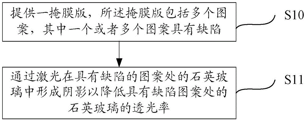
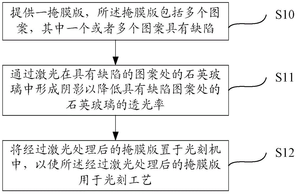
[0029] The post-processing method and usage method of the mask plate with defect patterns proposed by the present invention will be further described in detail below with reference to the accompanying drawings and specific embodiments. Advantages and features of the present invention will be apparent from the following description and claims. It should be noted that all the drawings are in a very simplified form and use imprecise scales, and are only used to facilitate and clearly assist the purpose of illustrating the embodiments of the present invention.

[0030] The core idea of ​​the present invention is to form a shadow in the quartz glass with the defective pattern by laser to reduce the light transmittance at the defective pattern, thereby avoiding the The formation of defect patterns on the wafer reduces the risk of defects in the wafer after the photolithography process, thereby reusing the mask with defects, avoiding repairing the mask with defects or remaking the ma...


PUM

PropertyMeasurementUnit
transmittivityaaaaaaaaaa

Abstract

The invention provides a post-processing method of a mask having a defect pattern; a shadow is formed in quartz glass at a position having a defect pattern by a laser so as to reduce the light transmittance of the position having the defect pattern, in the process of using the mask having the defect pattern for exposure, the defect pattern is avoided from being formed on a wafer, a risk of defect generation of the wafer after a photolithography technology is reduced, and a mask having the defect is reused, so as to avoid the problems of high manufacturing costs brought by repairing the mask having the defect or re-manufacturing a mask, namely reduce the manufacturing costs; and at the same time, the production yield is improved.

Description

technical field [0001] The invention relates to the technical field of integrated circuits, in particular to a post-processing method and using method of a mask plate with defect patterns. Background technique [0002] With the development of the semiconductor manufacturing process, the area of ​​the semiconductor chip is getting smaller and smaller, so the precision of the semiconductor process becomes more important. In the semiconductor manufacturing process, one of the important processes is photolithography, which is the process of transferring the pattern on the mask to the photolithography pattern on the wafer, so the quality of photolithography will directly affect the final formed chip performance. [0003] Usually, the mask contains a variety of patterns, mainly including: device patterns for forming functional devices, yield test patterns for yield testing, and window inspections for lithography processes A line or island pattern (sub-rule pattern) that is small...

Claims


Application Information

Patent Timeline
Patent Type & Authority Applications(China)
IPC IPC(8): G03F1/80
CPCG03F1/80G03F1/72
Inventor 胡华勇
Owner SEMICON MFG INT (SHANGHAI) CORP
Why Eureka
Try Eureka