Check patentability & draft patents in minutes with Patsnap Eureka AI!

EEPROM memory cell gate control signal generating circuit

A technology for controlling signals and memory cells, applied in information storage, static memory, read-only memory, etc., can solve the problems of high voltage, drains cannot be directly connected together, etc., to save costs and simplify circuits.

Active Publication Date: 2015-09-09
SHANGHAI HUAHONG GRACE SEMICON MFG CORP
View PDF3 Cites 2 Cited by
  • Summary
  • Abstract
  • Description
  • Claims
  • Application Information

AI Technical Summary

Problems solved by technology

However, the drains of PMOS transistors P0 and P1 and NMOS transistors N0 and N1 cannot be directly connected together, otherwise when the drains of PMOS transistors P0 and P1 output VPOS, VNEG will appear on the gates of NMOS transistors N0 and N1, causing the NMOS transistor The voltage of the gate oxide layer of N0 and N1 is too high; and when the drains of NMOS transistors N0 and N1 output VNEG, VPOS will appear in the gate of PMOS transistor P0 or P1, so that the voltage of the gate oxide layer of PMOS transistor P0 or P1 too high

Method used


Image

  • EEPROM memory cell gate control signal generating circuit
  • EEPROM memory cell gate control signal generating circuit
  • EEPROM memory cell gate control signal generating circuit

Examples


Embodiment Construction

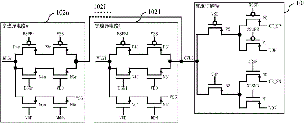
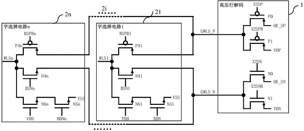
[0033] Such as figure 2 Shown is the circuit diagram for generating the gate control signal of the EEPROM storage unit according to the embodiment of the present invention. The EEPROM storage unit gate control signal generation circuit in the embodiment of the present invention includes:

[0034] High-voltage line decoding circuit 1 and multiple word selection circuits, such as word selection circuit 1 to word selection circuit n are marked with 21 to 2n respectively, wherein 2i marks word selection circuit i, and i represents any value in 1 to n.

[0035] The high-voltage row decoding circuit 1 includes a first partial row decoding circuit composed of a first PMOS transistor P0 and a second PMOS transistor P1, and a second partial row decoding circuit composed of a first NMOS transistor N0 and a second NMOS transistor N1.

[0036]The drain of the first PMOS transistor P0 is connected to the drain of the second PMOS transistor P1 and outputs the first total word line voltage...


PUM


Abstract

The invention discloses an EEPROM memory cell gate control signal generating circuit which comprises a high-voltage row decoding circuit and a plurality of word selection circuits, wherein the output of the high-voltage row decoding circuit is divided into two paths which are used for outputting first total word line voltage for providing positive erasing voltage and second total word line voltage for providing negative erasing voltage; the first total word line voltage and the second total word line voltage are input to each word selection circuit. Therefore, impact of positive erasing voltage on the gate oxide layers of NMOS transistors and impact of negative erasing voltage on PMOS transistors are avoided, and the number of MOS transistors used for isolating the gate oxide layers is decreased, that is, the circuit can be simplified, and the cost can be reduced.

Description

technical field [0001] The invention relates to a semiconductor integrated circuit, in particular to an EEPROM storage unit gate control signal generating circuit. Background technique [0002] Based on the EEPROM structure of the SONOS tube, the requirements for the gate voltage of the memory cell, that is, the word line voltage WLS, and the memory cell substrate VBULK are shown in Table 1: [0003] Table I [0004] [0005] Among them, VPOS is the positive voltage for erasing and writing, which is the positive high voltage required for erasing and programming, and VNEG is the negative voltage for erasing and writing, which is the negative high voltage required for erasing and programming. When programming, add VPOS and VNEG to the gate and substrate of the selected memory cell, respectively, for programming operation; add VNEG to the gate and substrate of unselected memory cells in the same column as the selected memory cell, and will not perform programming operation....

Claims


Application Information

Patent Timeline
IPC IPC(8): G11C16/14
CPCG11C16/08G11C5/06G11C16/10G11C16/12G11C16/14G11C16/16G11C16/24G11C16/26G11C16/30
Inventor 冯国友赵艳丽
Owner SHANGHAI HUAHONG GRACE SEMICON MFG CORP
Features
  • R&D
  • Intellectual Property
  • Life Sciences
  • Materials
  • Tech Scout
  • Unparalleled Data Quality
  • Higher Quality Content
  • 60% Fewer Hallucinations
Learn More