
Stacked module heat radiation structure and manufacturing method thereof

A heat dissipation structure and module technology, which is applied in the production of stacked module heat dissipation structure and the field of stacked module heat dissipation structure, can solve the problems of high chip temperature in the package, exceeding thermal specifications, complex structure, etc., and achieve easy operation and thermal resistance. Reduced, easy-to-step effects

Inactive Publication Date: 2015-09-09
NAT CENT FOR ADVANCED PACKAGING
View PDF3 Cites 3 Cited by
  • Summary
  • Abstract
  • Description
  • Claims
  • Application Information

AI Technical Summary

Problems solved by technology

[0003] However, PoP packaging usually adopts a two-layer package stacking structure. This vertical stacking makes the PoP package structure more complicated, and the air fluidity between the upper and lower packages becomes poor. The heat dissipation of the PoP package is mainly through the upper package. and the bottom substrate as the main path, resulting in poor heat dissipation performance of the PoP package
Especially in today's high-frequency mobile devices, the continuous increase of chip power consumption makes the heat dissipation problem of PoP more serious, and it is easy to cause the temperature of the chip in the package to be too high and exceed the requirements of thermal specifications.

Method used


Image

  • Stacked module heat radiation structure and manufacturing method thereof
  • Stacked module heat radiation structure and manufacturing method thereof
  • Stacked module heat radiation structure and manufacturing method thereof

Examples


Embodiment Construction

[0037] The present invention will be further described below in conjunction with specific examples.

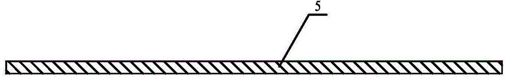
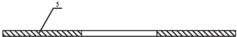
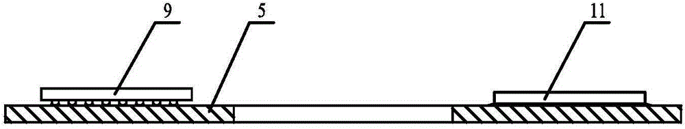
[0038] The heat dissipation structure of the stacked module includes a lower package substrate 1, a second solder ball 2, a second potting compound 3, a third chip 4, an upper package substrate 5, a first solder ball 6, a plastic package 7, a first potting Sealing glue 8, first chip 9, heat sink 10, second chip 11 and lead wire 12, described heat sink 10 has integrated base, is provided with the protruding part that protrudes downward on the lower surface of this base; The lower surface of the packaging substrate 1 is soldered with a second solder ball 2, and the third chip 4 is fixed on the middle of the upper surface of the lower packaging substrate 1 through the second potting glue 3, and an upper packaging substrate is arranged above the lower packaging substrate 1. 5. A window is opened in the middle of the upper packaging substrate 5, and a first solder ball 6 is welded ...


PUM

PropertyMeasurementUnit
Thicknessaaaaaaaaaa

Abstract

The invention discloses a stacked module heat radiation structure and a manufacturing method thereof. Second tin balls are welded on the lower surface of a lower packaging substrate. A third chip is fixed at the middle position of the upper surface of the lower packaging substrate. An upper packaging substrate is arranged above the lower packaging substrate. The middle position of the upper packaging substrate is provided with a window. First tin balls are welded on the lower surface of the upper packaging substrate. The first tin balls contact with the upper surface of the lower packaging substrate. The upper surface of the upper packaging substrate is provided with a plastic sealing member. A first chip is fixed on the upper surface of the upper packaging substrate at an inner position which corresponds with the plastic sealing member through first sealing glue. The projection of the base of a heat radiating plate penetrates through the window of the upper packaging substrate and is fixed with the upper surface of the third chip. According to the stacked module heat radiation structure, thermal resistance is reduced through the heat radiating plate structure, and a problem of overhigh temperature of the PoP can be effectively prevented.

Description

technical field [0001] The invention discloses a stacked module heat dissipation structure, and also discloses a manufacturing method of the stacked module heat dissipation structure, which belongs to the technical field of chip packaging. Background technique [0002] PoP (Package on Package) is a typical three-dimensional packaging solution, which can integrate logic chips and memory chips at the same time, and has become an important part of the handheld device market that is constantly pursuing smaller and thinner devices. Compared with the packaging form of chip stacking, the advantage of PoP packaging is that each device can be tested separately before assembly, which ensures a higher yield rate and the total stacking assembly cost can be minimized. At the same time, there is greater freedom in the choice of device combinations, and it is the preferred assembly solution for mobile phones, digital cameras and other products. [0003] However, PoP packaging usually adop...

Claims


Application Information

Patent Timeline
IPC IPC(8): H01L23/367H01L21/48
CPCH01L2224/16225H01L2224/48095H01L2224/48227H01L2224/73204H01L2224/73253H01L2224/73265H01L2924/15311H01L2924/1815
Inventor 孙鹏徐健周鸣昊
Owner NAT CENT FOR ADVANCED PACKAGING
Features
  • Generate Ideas
  • Intellectual Property
  • Life Sciences
  • Materials
  • Tech Scout
  • Unparalleled Data Quality
  • Higher Quality Content
  • 60% Fewer Hallucinations
Learn More