Eureka AIR delivers breakthrough ideas for toughest innovation challenges, trusted by R&D personnel around the world.

Lead frame and chip packaging structure

A technology of chip packaging structure and lead frame, which is applied in the direction of semiconductor devices, semiconductor/solid-state device components, electrical components, etc., can solve the problems of limited lead frame appearance, increased power supply noise interference, and inability to control characteristic impedance. Achieve the effects of improving electrical quality, improving electrical quality, and reducing the number of pins

Active Publication Date: 2015-09-09
ALICORP
View PDF4 Cites 2 Cited by
  • Summary
  • Abstract
  • Description
  • Claims
  • Application Information

AI Technical Summary

Problems solved by technology

However, this package structure cannot provide a flat ground plane due to the limited shape of the lead frame.
Therefore, the lead frame package structure cannot control the characteristic impedance of its circuit, nor can it provide a good current return path, which makes it difficult for the lead frame package structure to achieve the electrical quality required by high-frequency products in practical applications.
In addition, with the rapid development of large-scale and multi-functional integrated circuits, the number of pins in the above-mentioned lead frame also increases, thus increasing the interference of power supply noise

Method used


Image

  • Lead frame and chip packaging structure
  • Lead frame and chip packaging structure
  • Lead frame and chip packaging structure

Examples


Embodiment Construction

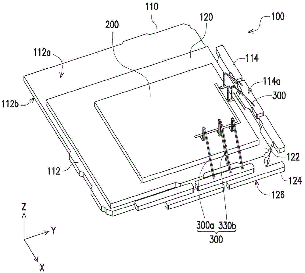
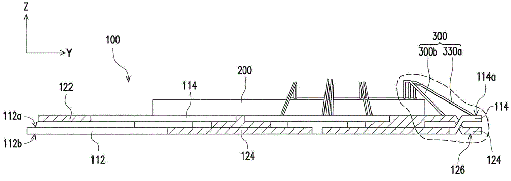
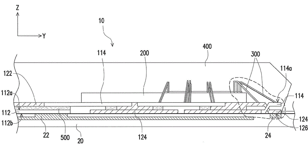
[0049] figure 1 is a schematic diagram of a lead frame according to an embodiment of the present invention. figure 2 It is a schematic side view of a lead frame according to an embodiment of the present invention. image 3 It is a schematic side view of a chip packaging structure according to an embodiment of the present invention. Please also refer to Figure 1 to Figure 3 , the lead frame 100 of this embodiment can be as figure 1 as well as figure 2 Shown to carry chip 200, to form as image 3 The chip package structure 10 shown is electrically connected with a circuit board 20 , for example. The chip package structure 10 can be as image 3 It includes a lead frame 100 , a chip 200 , a plurality of bonding wires 300 and an encapsulant 400 . In this embodiment, the circuit board 20 may include a ground pad 22 and a power pad 24, and the ground electrode plate 110 and the power electrode plate 120 may be electrically connected to the ground pad 22 and the power pad 24...


PUM


Abstract

A lead frame is suitable for bearing a chip and comprises a grounding electrode plate and a power supply electrode plate. The grounding electrode plate comprises a grounding electrode and at least one grounding extension portion. The grounding electrode has a first surface and a second surface opposite to the first surface. The grounding extension portion is connected with the grounding electrode and extends to the direction away from the first surface. The power supply electrode plate comprises a power supply electrode and at least one power supply extension portion. The power supply electrode is arranged above the grounding electrode and is parallel to the grounding electrode. The power supply extension portion is connected with the power supply electrode and extends to the direction approaching to the second surface. The chip is suitable for being arranged above the power supply electrode and is electrically connected with the grounding electrode plate and the power supply electrode plate.

Description

technical field [0001] The present invention relates to a lead frame and a semiconductor package structure, and in particular to a lead frame and a chip package structure using the lead frame. Background technique [0002] A semiconductor chip usually does not exist alone, but is connected to other chips and circuits through an I / O interface, and the internal circuit of a semiconductor chip is very complicated, requiring a chip package (package) to protect and carry it. The main functions of the chip package include: providing a current path to drive the circuit on the chip, distributing the signals entering and leaving the chip, dissipating the heat generated by the circuit to the outside world, and protecting the chip in a destructive environment. [0003] Nowadays, there are various types of carriers used in chip packaging, including lead frames, circuit substrates, etc., and various packaging structures can be formed. In recent years, the integration level of semiconduc...

Claims


Application Information

Patent Timeline
Patent Type & Authority Applications(China)
IPC IPC(8): H01L23/495H01L23/31
CPCH01L2224/48091H01L2224/48247H01L2924/00014
Inventor 林金松蔡嘉欣
Owner ALICORP
Why Eureka
Eureka Blog
Learn More