Method and device for digital filtering and dejittering
A digital filtering and de-jittering technology, applied in the direction of pulse shaping, etc., can solve the problems of difficult design, poor effect, high power consumption, etc., and achieve the effect of simple structure, low power consumption, and filter out burrs
- Summary
- Abstract
- Description
- Claims
- Application Information
AI Technical Summary
Problems solved by technology
Method used
Image
Examples
Embodiment 1
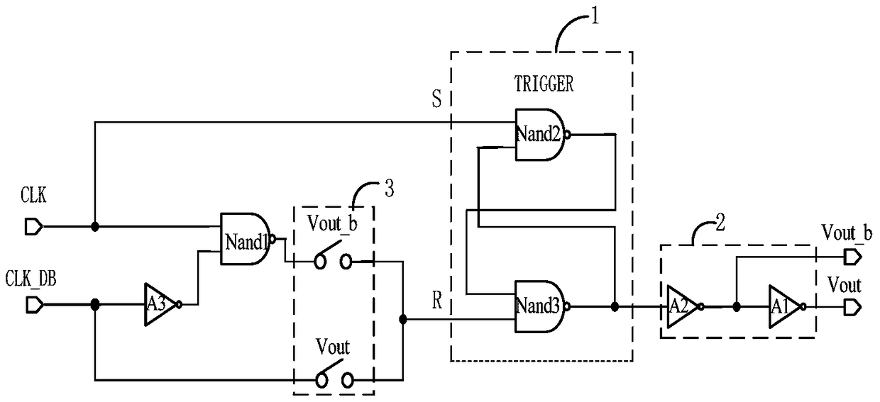
[0046] The present invention adopts the working principle of the flip-flop 1. According to the flip-flop 1, the reset signal of the reset terminal R of the flip-flop 1 is different from the holding signal of the holding terminal S to filter and de-jitter the clock input signal flowing into the flip-flop 1 . Specifically:
[0047] When the reset terminal R of the flip-flop 1 is at a low level, the initial clock output signal of the flip-flop 1 is at a high level, and the first clock output signal Vout is at a high level, and the second clock output signal Vout_b is a low level; when the reset terminal R of the flip-flop 1 is high and its holding terminal S is low, the flip-flop 1 flips, making the first clock output signal Vout low, The second clock output signal Vout_b is at a high level.
[0048] At the same time, when the feedback clock output signal is input to the feedback control circuit 3, the closing and opening of the corresponding switch is controlled by the level of the...
Embodiment 2
[0061] The second clock input signal CLK_DB is an inverted and delayed output clock signal of the first clock input signal CLK, where the glitch Δt between the second clock input signal CLK_DB and the first clock input signal CLK must be It is satisfied that Δt is greater than zero, and the glitches of the second clock input signal CLK_DB are made to be the first clock input signal CLK without overlapping each other.
[0062] Such as Figure 4 Shown is an output timing diagram of a digital filtering and de-jittering device in an embodiment of the present invention.
Embodiment 3
[0064] When the input first clock input signal CLK is at a logic high level, the delay unit 4Delay_Cell outputs the second clock input signal CLK_DB at a logic low level, and the first clock output signal Vout is an output signal with jitter removed.
[0065] Assuming that the initial output state of the flip-flop 1 is logic zero, the output of the second inverter A2 is logic high, and the output of the first NAND gate Nand1 is connected to the input of the flip-flop 1, at this time the first The NAND gate Nand1 is at a logic low level, so that the output of the flip-flop 1 is forced to be at a logic high level, and the second clock output signal output by the second inverter A2 is at a logic low level. The first clock output signal output by the device A1 is at a logic high level, and the connection between the first NAND gate Nand1 and the flip-flop 1TRIGGER is then disconnected, and the delay unit 4Delay_Cell outputs the clock signal CLK_DB and the flip-flop 1TRIGGER is connec...
PUM
 Abstract
Description
Claims
Application Information


