
Light emitting device and method for manufacturing the same

A light-emitting device and manufacturing method technology, applied in the field of Zener diodes and light-emitting devices, to achieve the effect of reducing the size of the frame

Active Publication Date: 2015-09-16
TOYODA GOSEI CO LTD
View PDF5 Cites 3 Cited by
  • Summary
  • Abstract
  • Description
  • Claims
  • Application Information

AI Technical Summary

Problems solved by technology

Second, there is also a gap between the ZD55 and the wiring pattern 52 due to the bump 59

Method used


Image

  • Light emitting device and method for manufacturing the same
  • Light emitting device and method for manufacturing the same
  • Light emitting device and method for manufacturing the same

Examples


Embodiment 1

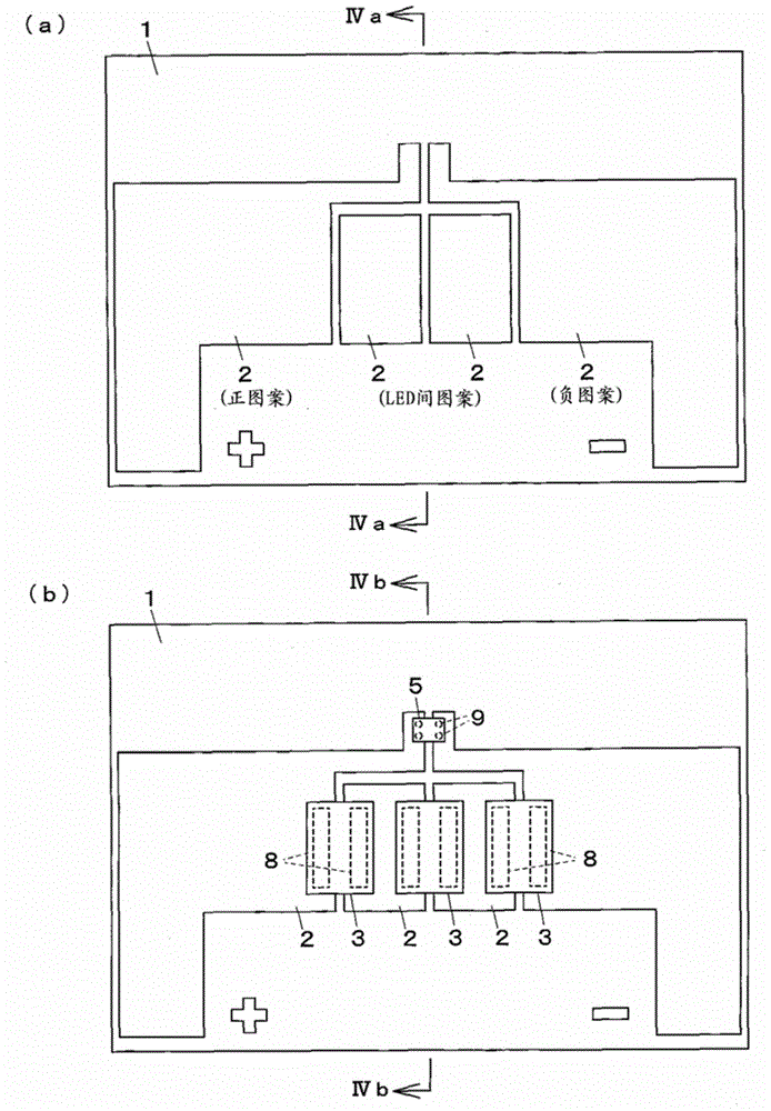
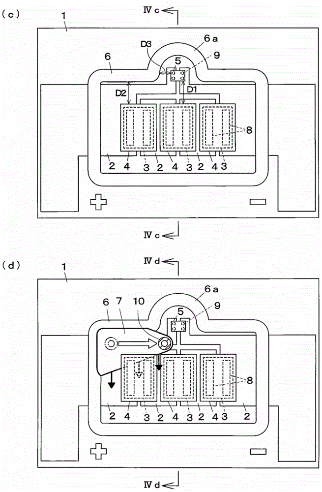
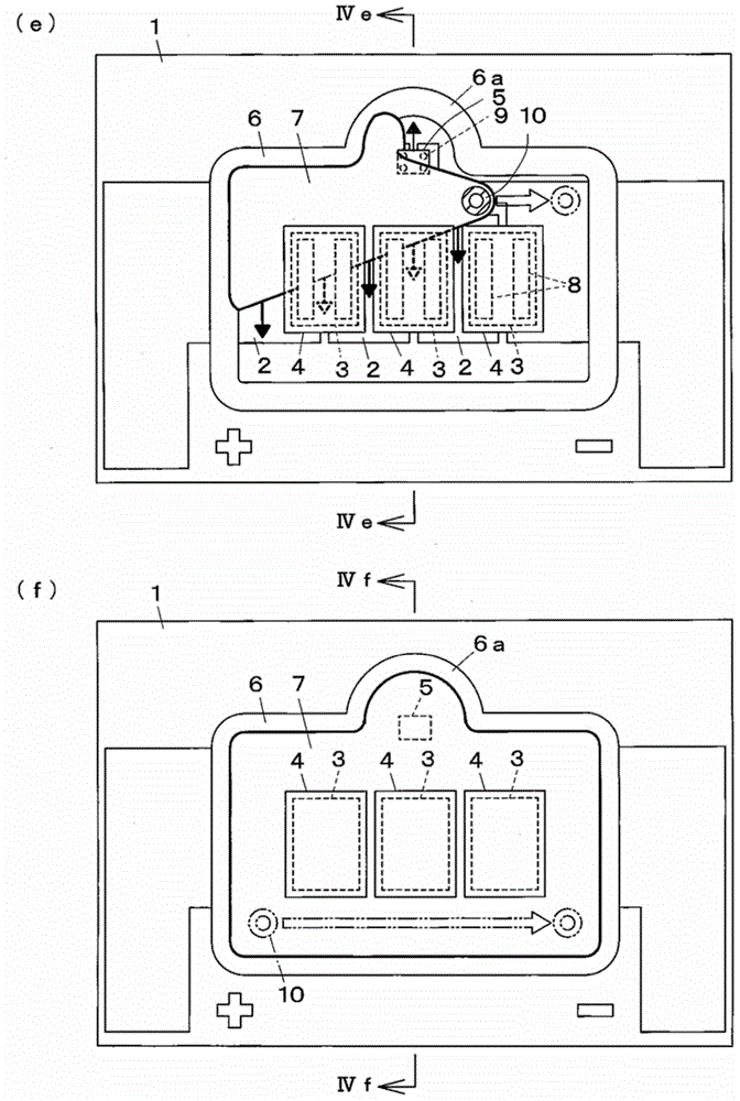
[0085] Below, refer to Figure 1 to Figure 6 Embodiment 1 in which the present invention is embodied in, for example, a light emitting device used as a light source of a headlight of an automobile will be described.

[0086] The light-emitting device includes: a substrate 1 provided with a wiring pattern 2 on the upper surface; an LED 3 emitting blue light mounted on two wiring patterns 2 at a predetermined interval; Body light-transmitting phosphor plate 4; ZD5 as a protective element of LED3 mounted on two wiring patterns 2 at a predetermined interval and next to LED3; surrounding LED3 formed on substrate 1 and the frame-shaped dam material 6 of ZD5; ​​and the light-reflective resin 7 injected into the inner side of the dam material 6, covering the side surfaces of the LED 3 and the phosphor plate 4, and covering the side surfaces and the upper surface of the ZD5.

[0087] The substrate 1 is made of a metal excellent in heat resistance and durability, such as AlN, and is, for...

Embodiment 2

[0114] For the light-emitting device of Example 2, such as Figure 7 (a) shows the state before injecting the light-reflective resin 7, only a part of the dam 6 (central portion of one long side) is formed in a V-shape bulging outward, and a third distance is separated. It is different from Embodiment 1 in that it surrounds the three sides of ZD5. Others are the same as in Example 1, and the light-reflective resin 7 is injected in the same manner as in Example 1.

Embodiment 3

[0116] For the light-emitting device of Example 3, such as Figure 7 (b) shows the state before injecting the light-reflective resin 7, only a part of the dam 6 (one end of one long side) is formed in a U-shaped shape that bulges outward, and the second It is different from Example 1 in that the three sides of ZD5 are surrounded by three distances. Others are the same as in Example 1, and the light-reflective resin 7 is injected in the same manner as in Example 1.


PUM


Abstract

A light emitting device includes a substrate, a light-emitting diode chip mounted on the substrate, a Zener diode chip mounted next to the light-emitting diode chip on the substrate, a frame-like dam material formed on the substrate to surround the light-emitting diode chip and the Zener diode chip, and a light-reflective resin injected inside the dam material to coat side surfaces of the light-emitting diode chip and side surfaces and an upper surface of the Zener diode chip. A part of the frame-like dam material swells outward to surround three of the side surfaces of the Zener diode chip.

Description

technical field [0001] The present invention relates to a light-emitting device including a light-emitting diode (LED) and a Zener diode (ZD) as a protective element thereof, and covering the side surfaces of the light-emitting diode (LED) with a light-reflective resin. In addition, in this specification, the LED chip may be simply referred to as "LED", the ZD chip may be simply referred to as "ZD", and both the LED chip and the ZD chip may be collectively referred to as "chip". Background technique [0002] In recent years, the scope of application of LEDs has rapidly expanded, and they are also used in automobile headlights. For headlamps, not only high brightness but also specific light distribution are required. In order to control this light distribution, a light-emitting device in which the side surfaces of LEDs are covered with a light-reflective resin has been proposed. [0003] For example, if Figure 14 As shown, the light-emitting device described in Patent Docu...

Claims


Application Information

Patent Timeline
IPC IPC(8): H01L33/54H01L33/56H05B44/00
CPCH01L2933/0041H01L25/0753H01L25/165H01L33/60H01L33/505H01L2933/005H01L2933/0058H05B33/089H01L29/866H01L25/167H01L33/54H01L33/56H01L2924/181H01L2224/16225H01L2924/00012H01L33/46
Inventor 和田聪福井康生野野川贵志
Owner TOYODA GOSEI CO LTD
Learn More